ꢀ ꢁ ꢂꢃ ꢄꢅꢆ ꢂ ꢇ ꢈ ꢀ ꢁ ꢂꢃ ꢄꢅ ꢆ ꢂꢉ
ꢄ ꢊꢋꢌꢅ ꢊꢄꢍꢀ ꢎꢏ ꢐꢉ ꢎ ꢐꢌꢑ ꢒꢏ ꢏ ꢓ ꢔ ꢕꢀꢓ ꢖꢕ ꢒꢄ ꢏ ꢓꢉ ꢗꢗ ꢏꢖ ꢏꢘꢍ ꢉꢀ ꢄ ꢄ ꢉꢘꢏ ꢖꢏꢇ ꢏꢉꢅ ꢏꢖ
SLLS202E − MAY 1995 − REVISED JUNE 2005
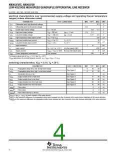
electrical characteristics over recommended supply-voltage and operating free-air temperature
ranges (unless otherwise noted)
†
PARAMETER
Differential input high-threshold voltage
Differential input low-threshold voltage
Enable input clamp voltage
High-level output voltage
Low-level output voltage
High-impedance-state output current
High-level enable input current
Low-level enable input current
Input resistance
TEST CONDITIONS
MIN TYP
MAX
UNIT
V
V
V
V
V
V
0.2
IT+
IT−
IK
−0.2
V
I = −18 mA
−0.8
3.2
−1.5
V
I
V
V
V
V
V
= 200 mV,
I
I
= −5 mA
= 5 mA
2.4
V
OH
OL
ID
OH
= −200 mV,
0.17
0.5
50
V
ID
OL
I
I
I
= 0 to V
CC
µA
OZ
O
= 0 or 3 V,
= 3.6 V,
V = 5.5 V
10
IH(E)
IL(E)
CC
CC
I
µA
V = 0 V
I
−10
r
7
12
kΩ
µA
mA
pF
I
I
I
Input current
V = 5.5 V or −0.3 V, All other inputs GND
700
17
I
I
Supply current
V
= V
CC
or GND, No load, line inputs open
8
CC
I(E)
One channel
‡
C
Power dissipation capacitance
150
pd
†
‡
All typical values are at V
CC
pd
= 3.3 V and T = 25°C.
A
C
determines the no-load dynamic current: I = C × V
× f + I .
CC
S
pd
CC
switching characteristics, V
= 3.3 V, T = 25°C
A
CC
PARAMETER
TEST CONDITIONS
MIN
8
TYP
16
16
5
MAX
20
UNIT
t
t
t
t
t
t
t
t
t
t
Propagation delay time, low- to high-level output
Propagation delay time, high- to low-level output
PLH
PHL
t
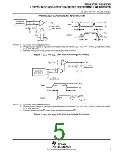
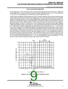
See Figure 1
ns
8
20
Transistion time (t or t )
See Figure 1
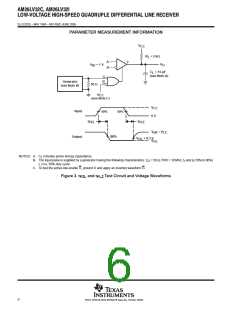
See Figure 2
See Figure 3
See Figure 2
See Figure 3
ns
ns
ns
ns
ns
ns
ns
ns
r
f
Output-enable time to high level
Output-enable time to low level
Output-disable time from high level
Output-disable time from low level
Pulse skew
17
10
20
16
4
40
40
40
40
6
PZH
PZL
PHZ
PLZ
sk(p)
sk(o)
§
¶
Pulse skew
4
6
#
Pulse skew (device to device)
6
9
sk(pp)
§
¶
#
t
t
t
is |t
− t | of each channel of the same device.
sk(p)
sk(o)
sk(pp)
PLH PHL
is the maximum difference in propagation delay times between any two channels of the same device switching in the same direction.
is the maximum difference in propagation delay times between any two channels of any two devices switching in the same direction.
4
POST OFFICE BOX 655303 • DALLAS, TEXAS 75265

 TI [ TEXAS INSTRUMENTS ]