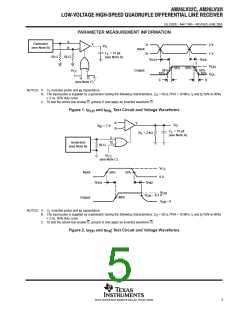
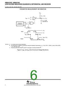
ꢀꢁ ꢂ ꢃ ꢄꢅꢆ ꢂ ꢇꢈ ꢀꢁ ꢂꢃ ꢄꢅ ꢆꢂ ꢉ
ꢄꢊ ꢋꢌꢅ ꢊꢄꢍꢀꢎ ꢏ ꢐꢉ ꢎ ꢐꢌꢑꢒ ꢏꢏꢓ ꢔ ꢕꢀꢓꢖ ꢕꢒꢄ ꢏ ꢓꢉ ꢗꢗ ꢏꢖ ꢏꢘꢍ ꢉꢀ ꢄ ꢄ ꢉꢘꢏ ꢖꢏ ꢇꢏ ꢉ ꢅꢏ ꢖ
SLLS202E − MAY 1995 − REVISED JUNE 2005
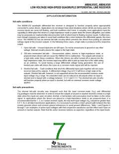
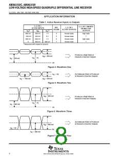
APPLICATION INFORMATION
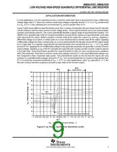
In most applications, it is not customary to have a common-mode input close to ground and to have a differential
voltage larger than 2 V. Since the common-mode input voltage is typically around 1.5 V, a 2-V V would result
ID
in a V of 0.5 V, thus satisfying the recommended V level of greater than 0.4 V.
IL
IL
Figure 8 plots seven different input threshold curves from a variety of production lots and shows how the fail-safe
circuitry behaves with the input common-mode voltage levels. These input threshold curves are representative
samples of production devices. The curves specifically illustrate a typical range of input threshold variation. The
AM26LV32 is specified with 200 mV of input sensitivity to account for the variance in input threshold. Each data
point represents the input’s ability to produce a known state at the output for a given V and V . Applying a
IC
ID
differential voltage at or above a certain point on a curve would produce a known state at the output. Applying
a differential voltage less than a certain point on a curve would activate the fail-safe circuit and the output would
be in a high state. For example, inspecting the top input threshold curve reveals that for a V + 1.6 V, V yields
IC
ID
around 87 mV. Applying 90 mV of differential voltage to this particular production lot generates a known receiver
output voltage. Applying a V of 80 mV activates the input fail-safe circuitry and the receiver output is placed
ID
in the high state. Texas Instruments specifies the input threshold at 200 mV, since normal process variations
affect this parameter. Note that at common-mode input voltages around 0.2 V, the input differential voltages are
low compared to their respective data points. This phenomenon points to the fact that the inputs are very
sensitive to small differential voltages around 0.2 V V . It is recommended that V levels be kept greater than
IC
IC
0.5 V to avoid this increased sensitivity at V [ 0.2 V. In most applications, since V typically is 1.5 V, the
IC
IC
fail-safe circuitry functions properly to provide a high state at the receiver output.
Most
Applications
100
90
80
70
60
Not
Recommended
50
40
30
20
10
0
Increased Receiver Input Sensitivity
0.2 0.4 0.6 0.8 1.2 1.4 1.6 1.8 2.2 2.4
−1 −0.8 −0.6 −0.4 −0.2
0
1
2
V
IC
− Common-Mode Input Voltage − V
Figure 8. V Versus V Receiver Sensitivity Levels
IC
ID
9
POST OFFICE BOX 655303 • DALLAS, TEXAS 75265

 TI [ TEXAS INSTRUMENTS ]