ADT7301
THEORY OF OPERATION
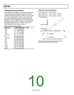
The ADT7301 is a 13-bit digital temperature sensor with a 14th
bit that acts as a sign bit. The part houses an on-chip temperature
sensor, a 13-bit A/D converter, a reference circuit, and serial
interface logic functions in SOT-23 and MSOP packages. The
ADC section consists of a conventional successive approximation
converter based around a capacitor DAC. The parts run on a
2.7 V to 5.25 V power supply.
The ADT7301 can be placed into shutdown mode via the control
register. This means that the on-chip oscillator is shut down and
no further conversions are initiated until the ADT7301 is taken
out of shutdown mode. The ADT7301 can be taken out of
shutdown mode by writing all 0s into the control register. The
conversion result from the last conversion prior to shutdown
can still be read from the ADT7301 even when it is in shutdown
mode.
The on-chip temperature sensor allows an accurate measure-
ment of the ambient device temperature to be made. The
specified measurement range of the ADT7301 is −40°C to
+150°C. Greater than 125°C, the ADT7301 is limited to 5%
of its 55°C operational lifetime. The structural integrity of the
device may start to deteriorate when continuously operated at
absolute maximum voltage and temperature specifications.
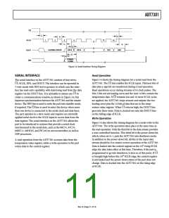
In normal conversion mode, the internal clock oscillator is reset
after every read or write operation. This causes the device to start
a temperature conversion, the result of which is typically available
1.2 ms later. Similarly, when the part is taken out of shutdown
mode, the internal clock oscillator is started and a conversion is
initiated. The conversion result is available 1.2 ms later. Every
result is stored in a buffer register and is loaded into the
temperature value register only at the first falling SCLK edge of
every serial port activity. Serial port activity does not interfere
with conversion processes, and every conversion is completed,
even during a read operation. A conversion has to be completed
before a read occurs, otherwise its result is not loaded into the
temperature value register and instead is loaded into the buffer
register. A new conversion is triggered at the end of each serial
port activity, except when a conversion is already in progress.
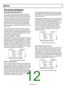
CONVERTER DETAILS
The conversion clock for the part is internally generated. No
external clock is required except when reading from and writing
to the serial port. In normal mode, an internal clock oscillator
runs an automatic conversion sequence. During this automatic
conversion sequence, a conversion is initiated every 1.5 second.
At this time, the part powers up its analog circuitry and performs
a temperature conversion. This temperature conversion typically
takes 1.2 ms, after which the analog circuitry of the part auto-
matically shuts down. The analog circuitry powers up again when
the 1.5 second timer times out and the next conversion begins.
Since the serial interface circuitry never shuts down, the result
of the most recent temperature conversion is always available in
the serial output register.
Rev. B | Page 9 of 16

 TI [ TEXAS INSTRUMENTS ]