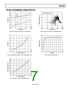
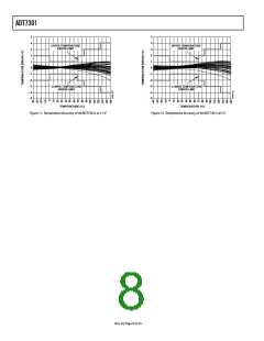
ADT7301
CS
t1
t7
t2
15
SCLK
2
3
4
1
16
t3
t8
t4
DB0
DB1
LEADING ZEROS
DB13
t6
DB12
DB0
DOUT
DIN
t5
POWER-
DOWN
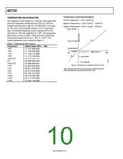
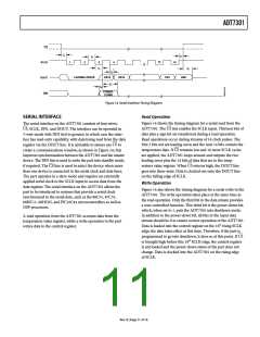
Figure 14. Serial Interface Timing Diagram
SERIAL INTERFACE
Read Operation
Figure 14 shows the timing diagram for a serial read from the
CS
The serial interface on the ADT7301 consists of four wires:
CS
ADT7301. The
line enables the SCLK input. Thirteen bits of
, SCLK, DIN, and DOUT. The interface can be operated in
data plus a sign bit are transferred during a read operation.
Read operations occur during streams of 16 clock pulses. The
first 2 bits out are leading zeros and the next 14 bits contain the
3-wire mode with DIN tied to ground, in which case the inter-
face has read-only capability, with data being read from the data
CS
register via the DOUT line. It is advisable to always use
to
CS
temperature data. If
remains low and 16 more SCLK cycles
create a communications window, as shown in Figure 14; this
improves synchronization between the ADT7301 and the master
device. The DIN line is used to write the part into standby mode,
CS
are applied, the ADT7301 loops around and outputs the two
leading zeros plus the 14 bits of data that are in the temp-
CS
erature value register. When
returns high, the DOUT line
if required. The
line is used to select the device when more
goes into three-state. Data is clocked out onto the DOUT line
on the falling edge of SCLK.
than one device is connected to the serial clock and data lines.
The part operates in a slave mode and requires an externally
applied serial clock to the SCLK input to access data from the
data register. The serial interface on the ADT7301 allows the
part to be interfaced to systems that provide a serial clock
synchronized to the serial data, such as the 80C51, 87C51,
68HC11, 68HC05, and PIC16Cxx microcontrollers as well as
DSP processors.
Write Operation
Figure 14 also shows the timing diagram for a serial write to the
ADT7301. The write operation takes place at the same time as
the read operation. Only the third bit in the data stream provides
a user-controlled function. This third bit is the power-down bit,
which, when set to 1, puts the ADT7301 into shutdown mode.
In addition to the power-down bit, all bits in the input data
stream should be 0 to ensure correct operation of the ADT7301.
Data is loaded into the control register on the 16th rising SCLK
edge; the data takes effect at this time. Therefore, if the part is
A read operation from the ADT7301 accesses data from the
temperature value register, while a write operation to the part
writes data to the control register.
CS
programmed to go into shutdown, it does so at this point. If
is brought high before this 16th SCLK edge, the control register
is not loaded and the power-down status of the part does not
change. Data is clocked into the ADT7301 on the rising edge
of SCLK.
Rev. B | Page 11 of 16

 TI [ TEXAS INSTRUMENTS ]