ADT7301
APPLICATIONS INFORMATION
MICROPROCESSOR INTERFACING
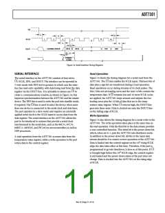
In the example shown in Figure 16, the ADT7301 is connected
to the serial port of the 8051. Because the serial interface of the
8051 contains only one data line, the DIN line of the ADT7301
is tied low in Figure 16.
The ADT7301 serial interface allows easy interface to most
microcomputers and microprocessors. Figure 15 to Figure 18
show some typical interface circuits. The serial interface on the
CS
ADT7301 consists of four wires: , DIN, DOUT, and SCLK.
For applications that require the ADT7301 power-down feature,
the serial interface should be implemented using data port lines
on the 8051. This allows a full-duplex serial interface to be
implemented. The method involves generating a serial clock on
one port line while using two other port lines to shift data
All interface circuits shown use all four interface lines. However,
it is possible to operate the interface with three wires. If the
application does not require the power-down facility offered
by the ADT7301, the DIN line can be tied low permanently.
Thus, the interface can be operated from just three wires: SCLK,
CS
in and out with the fourth port line connecting to . Port
CS
, and DOUT.
lines 1.0 to 1.3 (with P1.1 configured as an input) can be used
CS
to connect to SCLK, DOUT, DIN, and , respectively, to
implement this scheme.
The serial data transfer to and from the ADT7301 requires a
16-bit read operation. Many 8-bit microcontrollers have 8-bit
serial ports, and this 16-bit data transfer is handled as two 8-bit
transfers. Other microcontrollers and DSP processors transfer
16 bits of data in a serial data operation.
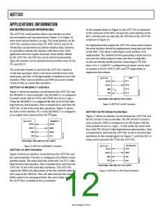
8051*
ADT7301*
P3.1
P3.0
P1.2
P1.3
SCLK
DOUT
DIN
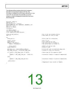
ADT7301-to-MC68HC11 Interface
Figure 15 shows an interface circuit between the ADT7301 and
the MC68HC11 microcontroller. The MC68HC11 is configured
in master mode with its CPOL and CPHA bits set to a Logic 1.
When the MC68HC11 is configured like this, its SCLK line idles
high between data transfers. Data is transferred to and from the
ADT7301 in two 8-bit serial data operations. Figure 15 shows
the full (4-wire) interface. PC1 of the MC68HC11 is configured
CS
*ADDITIONAL PINS OMITTED FOR CLARITY
Figure 16. ADT7301-to-8051 Interface
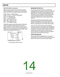
ADT7301-to-PIC16C6x/7x Interface
CS
as an output and is used to drive the
input.
Figure 17 shows an interface circuit between the ADT7301 and
the PIC16C6x/7x microcontroller. The PIC16C6x/7x synchro-
nous serial port (SSP) is configured as an SPI master with the
clock polarity bit set to a Logic 1. In this mode, the serial clock
line of the PIC16C6x/7x idles high between data transfers. Data
is transferred to and from the ADT7301 in two 8-bit serial data
operations. In the example shown in Figure 17, port line RA1 is
MC68HC11*
SCLK
ADT7301*
SCLK
DOUT
DIN
MISO
MOSI
PC1
CS
CS
being used to generate the
for the ADT7301.
*ADDITIONAL PINS OMITTED FOR CLARITY
PIC16C6x/7x*
SCK
ADT7301*
SCLK
Figure 15. ADT7301-to-MC68HC11 Interface
ADT7301-to-8051 Interface
SDO
SDI
DOUT
DIN
Figure 16 shows an interface circuit between the ADT7301 and
the microcontroller. The 8051 is configured in its Mode 0 serial
interface mode. The serial clock line of the 8051 (on P3.1) idles
high between data transfers. Data is transferred to and from the
ADT7301 in two 8-bit serial data operations. The ADT7301
outputs the MSB of its data stream as the first valid bit while the
8051 expects the LSB first. Thus, the data read into the serial
buffer needs to be rearranged before the correct data-word from
the ADT7301 is available in the accumulator.
RA1
CS
*ADDITIONAL PINS OMITTED FOR CLARITY
Figure 17. ADT7301-to-PIC16C6x/7x Interface
Rev. B | Page 12 of 16

 TI [ TEXAS INSTRUMENTS ]