ADT7301
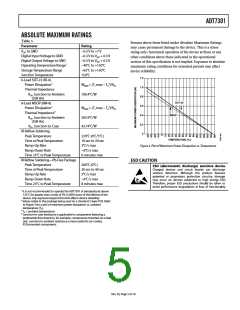
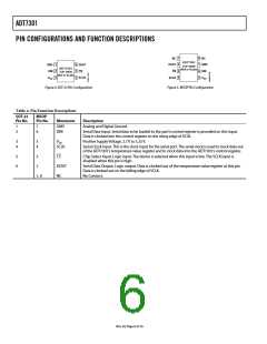
PIN CONFIGURATIONS AND FUNCTION DESCRIPTIONS
1
2
3
4
8
7
6
5
NC
DOUT
CS
NC
ADT7301
1
2
3
6
5
4
GND
DIN
DOUT
GND
DIN
TOP VIEW
(Not to Scale)
ADT7301
TOP VIEW
(Not to Scale)
CS
SCLK
V
SCLK
V
DD
DD
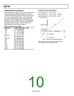
Figure 4. SOT-23 Pin Configuration
Figure 5. MSOP Pin Configuration
Table 4. Pin Function Descriptions
SOT-23
Pin No.
MSOP
Pin No.
Mnemonic
GND
DIN
Description
1
2
7
6
Analog and Digital Ground.
Serial Data Input. Serial data to be loaded to the part’s control register is provided on this input.
Data is clocked into the control register on the rising edge of SCLK.
3
4
5
4
VDD
SCLK
Positive Supply Voltage, 2.7 V to 5.25 V.
Serial Clock Input. This is the clock input for the serial port. The serial clock is used to clock data out
of the ADT7301’s temperature value register and to clock data into the ADT7301’s control register.
5
6
3
CS
Chip Select Input. Logic input. The device is selected when this input is low. The SCLK input is
disabled when this pin is high.
Serial Data Output. Logic output. Data is clocked out of the temperature value register at this pin.
Data is clocked out on the falling edge of SCLK.
2
DOUT
NC
1, 8
No Connect.
Rev. B | Page 6 of 16

 TI [ TEXAS INSTRUMENTS ]