ADS131M04-Q1
ZHCSOL7A –MARCH 2022 –REVISED AUGUST 2022
www.ti.com.cn
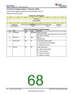
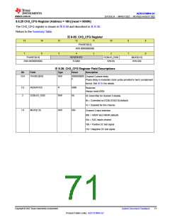
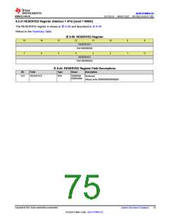
8.6.25 CH3_CFG Register (Address = 18h) [reset = 0000h]
The CH3_CFG register is shown in 图8-50 and described in 表8-38.
Return to the Summary Table.
图8-50. CH3_CFG Register
15
14
13
12
11
10
9
1
8
0
PHASE3[9:2]
R/W-0000000000b
7
6
5
4
3
2
PHASE3[1:0]
R/W-0000000000b
RESERVED
R-000b
DCBLK3_DIS0
R/W-0b
MUX3[1:0]
R/W-00b
表8-38. CH3_CFG Register Field Descriptions
Bit
Field
Type
Reset
Description
15:6
PHASE3[9:0]
R/W
0000000000
b
Channel 3 phase delay
Phase delay in modulator clock cycles provided in two's complement
format. See 表8-5 for details.
5:3
2
RESERVED
R
000b
0b
Reserved
Always reads 000b
DCBLK3_DIS0
R/W
DC block filter for channel 3 disable
0b = Controlled by DCBLOCK[3:0] (default)
1b = Disabled for this channel
1:0
MUX3[1:0]
R/W
00b
Channel 3 input selection
00b = AIN3P and AIN3N (default)
01b = ADC inputs shorted
10b = Positive DC test signal
11b = Negative DC test signal
Copyright © 2022 Texas Instruments Incorporated
Submit Document Feedback
71
Product Folder Links: ADS131M04-Q1

 TI [ TEXAS INSTRUMENTS ]