ADS131M04-Q1
ZHCSOL7A –MARCH 2022 –REVISED AUGUST 2022
www.ti.com.cn
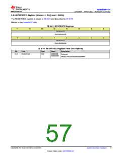
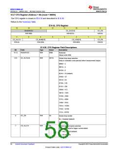
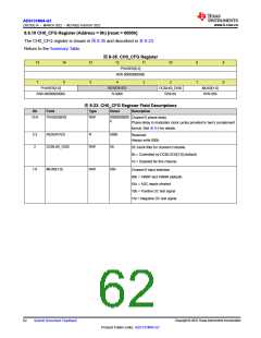
8.6.7 CFG Register (Address = 6h) [reset = 0600h]
The CFG register is shown in 图8-32 and described in 表8-20.
Return to the Summary Table.
图8-32. CFG Register
15
14
13
12
11
10
2
9
1
8
RESERVED
R/W-000b
GC_DLY[3:0]
R/W-0011b
GC_EN
R/W-0b
7
6
5
4
3
0
CD_ALLCH
R/W-0b
CD_NUM[2:0]
R/W-000b
CD_LEN[2:0]
R/W-000b
CD_EN
R/W-0b
表8-20. CFG Register Field Descriptions
Bit
Field
Type
Reset
Description
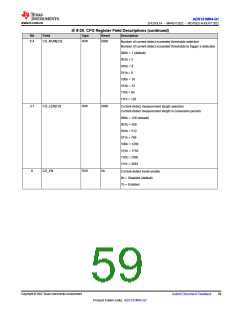
15:13
RESERVED
R/W
000b
Reserved
Always write 000b
12:9
GC_DLY[3:0]
R/W
0011b
Global-chop delay selection
Delay in modulator clock periods before measurement begins
0000b = 2
0001b = 4
0010b = 8
0011b = 16 (default)
0100b = 32
0101b = 64
0110b = 128
0111b = 256
1000b = 512
1001b = 1024
1010b = 2048
1011b = 4096
1100b = 8192
1101b = 16384
1110b = 32768
1111b = 65536
8
7
GC_EN
R/W
R/W
0b
0b
Global-chop enable
0b = Disabled (default)
1b = Enabled
CD_ALLCH
Current-detect channel selection
Channels required to trigger current-detect
0b = Any channel (default)
1b = All channels
Copyright © 2022 Texas Instruments Incorporated
58
Submit Document Feedback
Product Folder Links: ADS131M04-Q1

 TI [ TEXAS INSTRUMENTS ]