ADS131M04-Q1
ZHCSOL7A –MARCH 2022 –REVISED AUGUST 2022
www.ti.com.cn
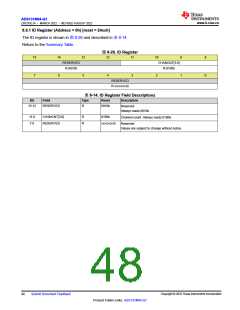
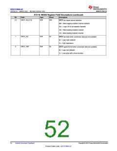
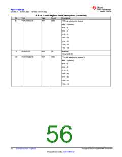
表8-16. MODE Register Field Descriptions (continued)
Bit
Field
Type
Reset
Description
3:2
DRDY_SEL[1:0]
R/W
00b
DRDY pin signal source selection
00b = Most lagging enabled channel (default)
01b = Logic OR of all enabled channels
10b = Most leading enabled channel
11b = Most leading enabled channel
1
0
DRDY_HiZ
R/W
R/W
0b
0b
DRDY pin state when conversion data are not available
0b = Logic high (default)
1b = High impedance
DRDY_FMT
DRDY signal format when conversion data are available
0b = Logic low (default)
1b = Low pulse with a fixed duration
Copyright © 2022 Texas Instruments Incorporated
52
Submit Document Feedback
Product Folder Links: ADS131M04-Q1

 TI [ TEXAS INSTRUMENTS ]