ADS131M04-Q1
ZHCSOL7A –MARCH 2022 –REVISED AUGUST 2022
www.ti.com.cn
8.3.3 Programmable Gain Amplifier (PGA)
Each channel of the ADS131M04-Q1 features an integrated programmable gain amplifier (PGA) that provides
gains of 1, 2, 4, 8, 16, 32, 64, and 128. The gains for all channels are individually controlled by the PGAGAINn
bits for each channel in the GAIN1 register.
Varying the PGA gain scales the differential full-scale input voltage range (FSR) of the ADC. 方程式 3 describes
the relationship between FSR and gain. 方程式 3 uses the internal reference voltage, 1.2 V, as the scaling factor
without accounting for gain error caused by tolerance in the reference voltage.
FSR = ±1.2 V / Gain
(3)
表8-1 shows the corresponding full-scale ranges for each gain setting.
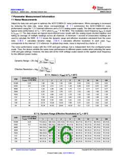
表8-1. Full-Scale Range
GAIN SETTING
FSR
1
2
±1.2 V
±600 mV
±300 mV
±150 mV
±75 mV
4
8
16
32
64
128
±37.5 mV
±18.75 mV
±9.375 mV
The input impedance of the PGA dominates the input impedance characteristics of the ADS131M04-Q1. The
PGA input impedance for gain settings up to 4 behaves according to 方程式 4 without accounting for device
tolerance and change over temperature. Minimize the output impedance of the circuit that drives the
ADS131M04-Q1 inputs to obtain the best possible gain error, INL, and distortion performance.
330 kΩ× 4.096 MHz / fMOD
(4)
where:
• fMOD is the ΔΣmodulator frequency, fCLKIN / 2
The device uses an input precharge buffer for PGA gain settings of 8 and higher. The input impedance at these
gain settings is very high. Specifying the input bias current for these gain settings is therefore more useful. A plot
of input bias current for the high gain settings is provided in 图6-5.
8.3.4 Voltage Reference
The ADS131M04-Q1 uses an internally generated, low-drift, band-gap voltage to supply the reference for the
ADC. The reference has a nominal voltage of 1.2 V, allowing the differential input voltage to swing from –1.2 V
to 1.2 V. The reference circuitry starts up very quickly to accommodate the fast start-up feature of this device.
The device waits until after the reference circuitry is fully settled before generating conversion data.
8.3.5 Clocking and Power Modes
An LVCMOS clock must be provided at the CLKIN pin continuously when the ADS131M04-Q1 is running in
normal operation. The frequency of the clock can be scaled in conjunction with the power mode to provide a
tradeoff between power consumption and dynamic range.
The PWR[1:0] bits in the CLOCK register allow the device to be configured in one of three power modes: high-
resolution (HR) mode, low-power (LP) mode, and very low-power (VLP) mode. Changing the PWR[1:0] bits
scales the internal bias currents to achieve the expected power levels. The external clock frequency must follow
the guidance provided in the Recommended Operating Conditions table corresponding to the intended power
mode in order for the device to perform according to the specification.
Copyright © 2022 Texas Instruments Incorporated
20
Submit Document Feedback
Product Folder Links: ADS131M04-Q1

 TI [ TEXAS INSTRUMENTS ]