ADS131M04-Q1
ZHCSOL7A –MARCH 2022 –REVISED AUGUST 2022
www.ti.com.cn
8 Detailed Description
8.1 Overview
The ADS131M04-Q1 is a low-power, four-channel, simultaneous-sampling, 24-bit, delta-sigma (ΔΣ) analog-to-
digital converter (ADC) with a low-drift internal reference voltage. The dynamic range, size, feature set, and
power consumption are optimized for cost-sensitive applications requiring simultaneous-sampling.
The ADS131M04-Q1 requires both analog and digital supplies. The analog power supply (AVDD – AGND) can
operate between 2.7 V and 3.6 V. An integrated negative charge pump allows absolute input voltages as low as
1.3 V below AGND, which enables measurements of input signals varying around ground with a single-ended
power supply. The digital power supply (DVDD – DGND) accepts both 1.8-V and 3.3-V supplies. The device
features a programmable gain amplifier (PGA) with gains up to 128. An integrated input precharge buffer
enabled at gains greater than 4 ensures high input impedance at high PGA gain settings. The ADC receives the
reference voltage from an integrated 1.2-V reference. The device allows differential input voltages as large as
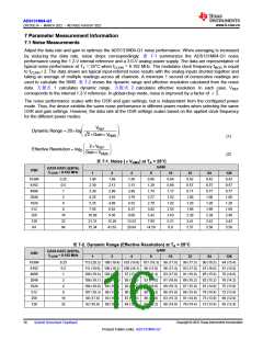
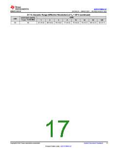
the reference. Three power-scaling modes allow designers to trade power consumption for ADC dynamic range.
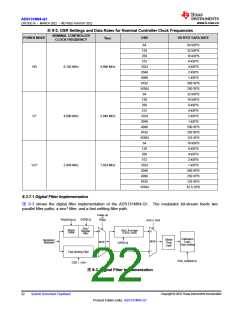
Each channel on the ADS131M04-Q1 contains a digital decimation filter that demodulates the output of the ΔΣ
modulators. The filter enables data rates as high as 32 kSPS per channel in high-resolution mode. The relative
phase of the samples can be configured between channels, thus enabling an accurate compensation for the
sensor phase response. Offset and gain calibration registers can be programmed to automatically adjust output
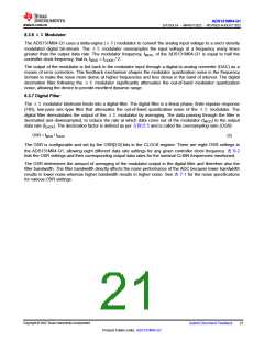
samples for measured offset and gain errors. The Functional Block Diagram provides a detailed diagram of the
ADS131M04-Q1.
The device communicates via a serial programming interface (SPI)-compatible interface. Several SPI commands
and internal registers control the operation of the ADS131M04-Q1. Other devices can be added to the same SPI
bus by adding discrete CS control lines. The SYNC/RESET pin can be used to synchronize conversions
between multiple ADS131M04-Q1 devices as well as to maintain synchronization with external events.
8.2 Functional Block Diagram
AVDD
DVDD
1.2-V
Reference
AIN0P
AIN0N
+
Phase Shift &
Digital Filters
Gain & Offset
Calibration
DS ADC
DS ADC
DS ADC
DS ADC
œ
SYNC / RESET
AIN1P
AIN1N
+
Phase Shift &
Digital Filters
Gain & Offset
Calibration
CS
œ
SCLK
Control &
Serial Interface
DIN
DOUT
DRDY
AIN2P
AIN2N
+
Phase Shift &
Digital Filters
Gain & Offset
Calibration
œ
Clock
Generation
CLKIN
AIN3P
AIN3N
+
Phase Shift &
Digital Filters
Gain & Offset
Calibration
œ
AGND
DGND
Copyright © 2022 Texas Instruments Incorporated
18
Submit Document Feedback
Product Folder Links: ADS131M04-Q1

 TI [ TEXAS INSTRUMENTS ]