ADS131M04-Q1
ZHCSOL7A –MARCH 2022 –REVISED AUGUST 2022
www.ti.com.cn
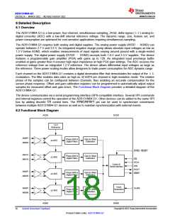
8.3 Feature Description
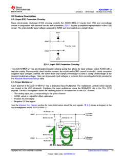
8.3.1 Input ESD Protection Circuitry
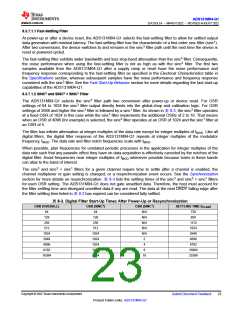
Basic electrostatic discharge (ESD) circuitry protects the ADS131M04-Q1 inputs from ESD and overvoltage
events in conjunction with external circuits and assemblies. 图8-1 depicts a simplified representation of the ESD
circuit. The protection for input voltages exceeding AVDD can be modeled as a simple diode.
AVDD
AINnP
To analog inputs
AINnN
AVDD
图8-1. Input ESD Protection Circuitry
The ADS131M04-Q1 has an integrated negative charge pump that allows for input voltages below AGND with a
unipolar supply. Consequently, shunt diodes between the inputs and AGND cannot be used to clamp excessive
negative input voltages. Instead, the same diode that clamps overvoltage is used to clamp undervoltage at the
reverse breakdown voltage. Take care to prevent input voltages or currents from exceeding the limits provided in
the Absolute Maximum Ratings table.
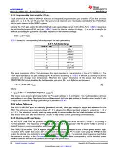
8.3.2 Input Multiplexer
Each channel of the ADS131M04-Q1 has a dedicated input multiplexer. The multiplexer controls which signals
are routed to the ADC channels. Configure the input multiplexer using the MUXn[1:0] bits in the CHn_CFG
register. The input multiplexer allows the following inputs to be connected to the ADC channel:
• The analog input pins corresponding to the given channel
• AGND, which is helpful for offset calibration
• Positive DC test signal
• Negative DC test signal
See the Internal Test Signals section for more information about the test signals. 图 8-2 shows a diagram of the
input multiplexer on the ADS131M04-Q1.
MUXn[1:0] = 00
SW
To Positive
PGA Input
AINnP
MUXn[1:0] = 01
MUXn[1:0] = 10
+
DC Test
Signal
œ
AGND
MUXn[1:0] = 11
MUXn[1:0] = 10
MUXn[1:0] = 01
SW
To Negative
PGA Input
AINnN
MUXn[1:0] = 00
图8-2. Input Multiplexer
Copyright © 2022 Texas Instruments Incorporated
Submit Document Feedback
19
Product Folder Links: ADS131M04-Q1

 TI [ TEXAS INSTRUMENTS ]