ADS131B04-Q1
ZHCSMK3B –NOVEMBER 2020 –REVISED NOVEMBER 2021
www.ti.com.cn
MAX UNIT
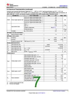
6.6 Timing Requirements
over operating ambient temperature range, and DOUT load = 20 pF || 100 kΩ (unless otherwise noted)
MIN
2.7 V ≤DVDD ≤3.6 V
tw(CLL)
tw(CLH)
tc(SC)
Pulse duration, CLKIN low
Pulse duration, CLKIN high
SCLK period
49
49
40
20
20
15
16
10
5
ns
ns
ns
tw(SCL)
tw(SCH)
tw(CSH)
Pulse duration, SCLK low
Pulse duration, SCLK high
Pulse duration, CS high
ns
ns
ns
td(CSSC) Delay time, first SCLK rising edge after CS falling edge
td(SCCS) Delay time, CS rising edge after final SCLK falling edge
ns
ns
tsu(DI)
th(DI)
Setup time, DIN valid before SCLK falling edge
ns
Hold time, DIN valid after SCLK falling edge
8
ns
ns
tsu(SY)
tw(SYL)
tw(RSL)
Setup time, SYNC/RESET valid before CLKIN rising edge
Pulse duration, SYNC/RESET low for synchronization
Pulse duration, SYNC/RESET low to generate device reset
10
1
2047 tMCLK
tMCLK
2048
6.7 Switching Characteristics
over operating ambient temperature range, and DOUT load = 20 pF || 100 kΩ (unless otherwise noted)
PARAMETER
TEST CONDITIONS
MIN
TYP
MAX UNIT
2.7 V ≤DVDD ≤3.6 V
Propagation delay time, CS falling edge to
DOUT driven
tp(CSDO)
tp(SCDO)
tp(CSDOZ)
50
20
75
ns
ns
ns
Progapation delay time, SCLK rising edge to
valid new DOUT
Propagation delay time, CS rising edge to
DOUT high impedance
tw(DRH)
tw(DRL)
Pulse duration, DRDY high
Pulse duration, DRDY low
SPI timeout
4
4
tMCLK
tMCLK
tMCLK
32768
Measured from supplies at 90%
to first DRDY rising edge
tPOR
Power-on-reset time
250
5
µs
µs
tREGACQ Register default acquisition time
Copyright © 2022 Texas Instruments Incorporated
8
Submit Document Feedback
Product Folder Links: ADS131B04-Q1

 TI [ TEXAS INSTRUMENTS ]