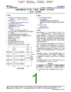
ADS131B04-Q1
ZHCSMK3B –NOVEMBER 2020 –REVISED NOVEMBER 2021
www.ti.com.cn
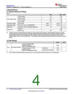
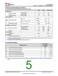
6 Specifications
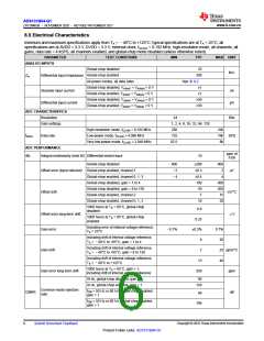
6.1 Absolute Maximum Ratings
See (1)
MIN
–0.3
MAX UNIT
AVDD to AGND
3.9
AGND to DGND
Power-supply voltage
0.3
V
3.9
–0.3
DVDD to DGND
–0.3
CAP to DGND
2.2
–0.3
Analog input voltage
Digital input voltage
Input current
AINxP, AINxN
AVDD + 0.3
V
V
AGND –1.6
DGND –0.3
–10
CS, CLKIN, DIN, SCLK, SYNC/RESET
Continuous, all pins except power-supply pins
Junction, TJ
DVDD + 0.3
10
150
150
mA
Temperature
°C
Storage, Tstg
–60
(1) Operation outside the Absolute Maximum Ratings may cause permanent device damage. Absolute Maximum Ratings do not imply
functional operation of the device at these or any other conditions beyond those listed under Recommended Operating Conditions. If
briefly operating outside the Recommended Operating Conditions but within the Absolute Maximum Ratings, the device may not
sustain damage, but it may not be fully functional –this may affect device reliability, functionality, performance, and shorten the device
lifetime.
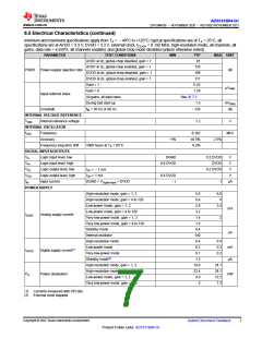
6.2 ESD Ratings
VALUE
UNIT
Human-body model (HBM),
per AEC Q100-002(1)
±2000
HBM ESD classification level 2
V(ESD)
Electrostatic discharge
V
Charged-device model (CDM),
per AEC Q100-011
CDM ESD classification level C4B
Corner pins
±750
±500
All other non-corner pins
(1) AEC Q100-002 indicates that HBM stressing shall be in accordance with the ANSI/ESDA/JEDEC JS-001 specification.
Copyright © 2022 Texas Instruments Incorporated
4
Submit Document Feedback
Product Folder Links: ADS131B04-Q1

 TI [ TEXAS INSTRUMENTS ]