ADS131B04-Q1
ZHCSMK3B –NOVEMBER 2020 –REVISED NOVEMBER 2021
www.ti.com.cn
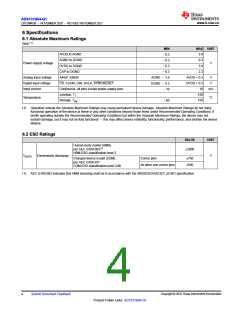
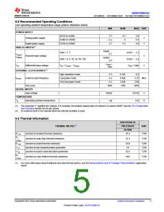
6.3 Recommended Operating Conditions
over operating ambient temperature range (unless otherwise noted)
MIN
NOM
MAX UNIT
POWER SUPPLY
AVDD to AGND
Analog power supply
2.7
–0.3
2.7
3.3
0
3.6
V
AGND to DGND
0.3
Digital power supply
DVDD to DGND
3.3
3.6
V
ANALOG INPUTS(1)
AGND –
Gain = 1, 2
AVDD –1.2
AVDD –2.4
VREF / Gain
0.1
VAINxP
VAINxN
,
Absolute input voltage
V
V
AGND –
Gain = 4, 8, 16, 32, 64, 128
VIN = VAINxP - VAINxN
0.3
–VREF
/
VIN
Differential input voltage
Gain
EXTERNAL CLOCK SOURCE(2)
High-resolution mode
Low-power mode
0.3
0.3
8.192
4.096
2.048
50%
8.2
fCLKIN
External clock frequency
4.15 MHz
2.08
Very-low-power mode
0.3
Duty cycle
40%
60%
DIGITAL INPUTS
Input voltage
TEMPERATURE
TA Operating ambient temperature
DGND
DVDD
V
125
°C
–40
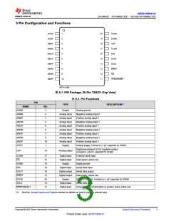
(1) The subscript "x" signifies the channel. For example, the positive analog input of channel 0 is named AIN0P. See the Pin Configuration
and Functions section for the pin names.
(2) An external clock is not required when the internal oscillator is used.
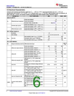
6.4 Thermal Information
ADS131B04-Q1
THERMAL METRIC(1)
PW (TSSOP)
20 PINS
91.5
UNIT
RθJA
Junction-to-ambient thermal resistance
°C/W
°C/W
Rθ
Junction-to-case (top) thermal resistance
31.4
JC(top)
RθJB
ΨJT
Junction-to-board thermal resistance
43.0
2.0
°C/W
°C/W
°C/W
Junction-to-top characterization parameter
Junction-to-board characterization parameter
42.5
ΨJB
Rθ
Junction-to-case (bottom) thermal resistance
N/A
°C/W
JC(bot)
(1) For more information about traditional and new thermal metrics, see the Semiconductor and IC Package Thermal Metrics application
report.
Copyright © 2022 Texas Instruments Incorporated
Submit Document Feedback
5
Product Folder Links: ADS131B04-Q1

 TI [ TEXAS INSTRUMENTS ]