ADS131B04-Q1
ZHCSMK3B –NOVEMBER 2020 –REVISED NOVEMBER 2021
www.ti.com.cn
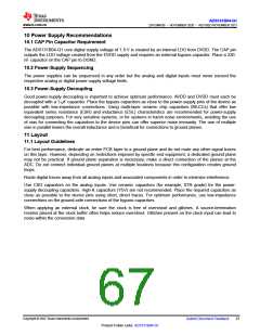
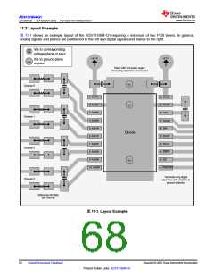
11.2 Layout Example
图 11-1 shows an example layout of the ADS131B04-Q1 requiring a minimum of two PCB layers. In general,
analog signals and planes are partitioned to the left and digital signals and planes to the right.
+3.3 V
Via to corresponding
voltage plane or pour
+3.3 V
+3.3 V
Via to ground plane
or pour
Place CAP and power supply
decoupling capacitors close to pins
Channel 0
1: AVDD
2: AGND
3: AIN0P
4: AIN0N
5: AIN1N
6: AIN1P
7: AIN2P
8: AIN2N
9: AIN3N
10: AIN3P
20: DVDD
19: DGND
18: CAP
Channel 1
Channel 2
Channel 3
17: CLKIN
16: DIN
Device
15: DOUT
14: SCLK
13: DRDY
12: CS
11: SYNC/RST
Terminate long digital
input lines with resistors to
prevent reflection
Differential RC-filter
per channel
图11-1. Layout Example
Copyright © 2022 Texas Instruments Incorporated
68
Submit Document Feedback
Product Folder Links: ADS131B04-Q1

 TI [ TEXAS INSTRUMENTS ]