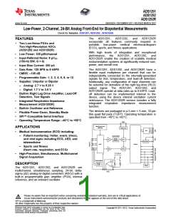
ADS1291
ADS1292
ADS1292R
www.ti.com
SBAS502A –DECEMBER 2011–REVISED MARCH 2012
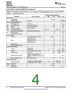
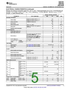
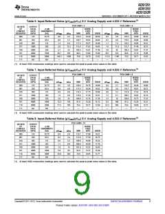
ELECTRICAL CHARACTERISTICS
Minimum and maximum specifications apply from –40°C to +85°C. Typical specifications are at +25°C. All specifications are
at DVDD = 1.8 V, AVDD – AVSS = 3 V(1), VREF = 2.42 V, external fCLK = 512 kHz, data rate = 500 SPS, CFILTER = 4.7 nF(2)
,
and gain = 6, unless otherwise noted.
ADS1291, ADS1292, ADS1292R
PARAMETER
TEST CONDITIONS
MIN
TYP
MAX
UNIT
ANALOG INPUTS
Full-scale differential input voltage
(AINP – AINN)
±VREF/GAIN
V
See the Input Common-Mode Range
subsection of the PGA Settings and Input
Range section
Input common-mode range
Input capacitance
20
pF
pA
nA
TA = +25°C, input = 1.5 V
±200
Input bias current (PGA chop = 8 kHz)
TA = –40°C to +85°C, input = 1.5 V
Chop rates other than 8 kHz
±1
See Pace Detect section
1000
No pull-up or pull-down current source
MΩ
MΩ
Current source lead-off detection (nA),
AVSS + 0.3 V < AIN < AVDD – 0.3 V
500
100
DC input impedance
Current source lead-off detection (µA),
AVSS + 0.6 V < AIN < AVDD – 0.6 V
MΩ
PGA PERFORMANCE
Gain settings
1, 2, 3, 4, 6, 8, 12
8.5
With a 4.7-nF capacitor on PGA output
(see PGA Settings and Input Range section
for details)
Bandwidth
kHz
ADC PERFORMANCE
Resolution
24
Bits
Data rate
fCLK = 512 kHz
125
8000
11
SPS
CHANNEL PERFORMANCE (DC Performance)
Gain = 6(3), 10 seconds of data
8
8
μVPP
μVPP
Gain = 6, 256 points, 0.5 seconds of data
Input-referred noise
Gain settings other than 6,
data rates other than 500 SPS
See Noise Measurements section
Integral nonlinearity
Offset error
Full-scale with gain = 6, best fit
2
±100
2
ppm
μV
Offset error drift
μV/°C
μV
Offset error with calibration
Gain error
15
Excluding voltage reference error
Excluding voltage reference drift
±0.1
2
±0.2
% of FS
ppm/°C
% of FS
Gain drift
Gain match between channels
CHANNEL PERFORMANCE (AC performance)
0.2
CMRR
PSRR
Common-mode rejection ratio
Power-supply rejection ratio
Crosstalk
fCM = 50 Hz and 60 Hz(4)
–105
–120
90
dB
dB
dB
dB
dB
dB
fPS = 50 Hz and 60 Hz
fIN = 50 Hz and 60 Hz
–120
107
SNR
THD
Signal-to-noise ratio
fIN = 10 Hz input, gain = 6
10 Hz, –0.5 dBFs, CFILTER = 4.7nF
100 Hz, –0.5 dBFs, CFILTER = 4.7nF
–104
–95
Total harmonic distortion
ADS1292R channel 1, 10 Hz, –0.5 dBFS,
CFILTER = 47 nF
–82
dB
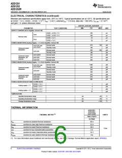
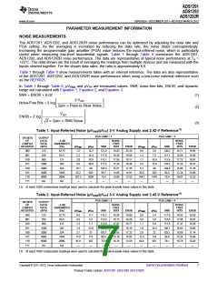
(1) Performance is applicable for 5-V operation as well. Production testing for limits is performed at 3 V.
(2) CFILTER is the capacitor accross the PGA outputs; see the PGA Settings and Input Range section for details.
(3) Noise data measured in a 10-second interval. Test not performed in production. Input-referred noise is calculated with input shorted
(without electrode resistance) over a 10-second interval.
(4) CMRR is measured with a common-mode signal of AVSS + 0.3 V to AVDD – 0.3 V. The values indicated are the minimum of the two
channels.
Copyright © 2011–2012, Texas Instruments Incorporated
Submit Documentation Feedback
3
Product Folder Link(s): ADS1291 ADS1292 ADS1292R

 TI [ TEXAS INSTRUMENTS ]