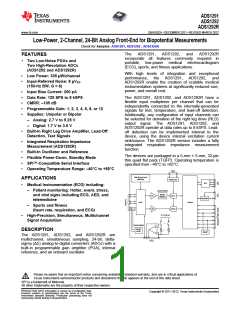
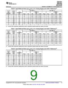
ADS1291
ADS1292
ADS1292R
SBAS502A –DECEMBER 2011–REVISED MARCH 2012
www.ti.com
This integrated circuit can be damaged by ESD. Texas Instruments recommends that all integrated circuits be handled with
appropriate precautions. Failure to observe proper handling and installation procedures can cause damage.
ESD damage can range from subtle performance degradation to complete device failure. Precision integrated circuits may be more
susceptible to damage because very small parametric changes could cause the device not to meet its published specifications.
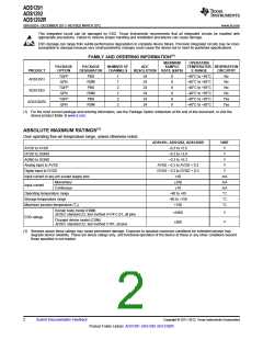
FAMILY AND ORDERING INFORMATION(1)
MAXIMUM
SAMPLE
RESOLUTION RATE (kSPS)
OPERATING
TEMPERATUR RESPIRATION
E RANGE
PACKAGE
OPTION
PACKAGE
DESIGNATOR
NUMBER OF
CHANNELS
ADC
PRODUCT
CIRCUITRY
TQFP
QFN
PBS
RSM
PBS
RSM
PBS
RSM
1
1
2
2
2
2
24
24
24
24
24
24
8
8
8
8
8
8
–40°C to +85°C
–40°C to +85°C
–40°C to +85°C
–40°C to +85°C
–40°C to +85°C
–40°C to +85°C
No
No
ADS1291I
TQFP
QFN
No
ADS1292I
No
TQFP
QFN
Yes
Yes
ADS1292RI
(1) For the most current package and ordering information, see the Package Option Addendum at the end of this document, or visit the
device product folder at www.ti.com.
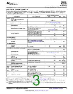
ABSOLUTE MAXIMUM RATINGS(1)
Over operating free-air temperature range, unless otherwise noted.
ADS1291, ADS1292, ADS1292R
UNIT
V
AVDD to AVSS
–0.3 to +5.5
DVDD to DGND
–0.3 to +3.9
V
AGND to DGND
–0.3 to +0.3
V
Analog input to AVSS
Digital input to DVDD
Input current to any pin except supply pins
AVSS – 0.3 to AVDD + 0.3
V
DVSS – 0.3 to DVDD + 0.3
V
±10
±100
mA
mA
mA
°C
°C
°C
Momentary
Input current
Continuous
±10
Operating temperature range
Storage temperature range
Maximum junction temperature (TJ)
Human body model (HBM)
–40 to +85
–60 to +150
+150
±1000
±500
V
V
JEDEC standard 22, test method A114-C.01, all pins
ESD ratings
Charged device model (CDM)
JEDEC standard 22, test method C101, all pins
(1) Stresses above these ratings may cause permanent damage. Exposure to absolute maximum conditions for extended periods may
degrade device reliability. These are stress ratings only, and functional operation of the device at these or any other conditions beyond
those specified is not implied.
2
Submit Documentation Feedback
Copyright © 2011–2012, Texas Instruments Incorporated
Product Folder Link(s): ADS1291 ADS1292 ADS1292R

 TI [ TEXAS INSTRUMENTS ]