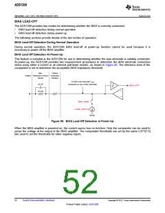
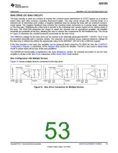
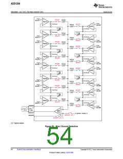
ADS1299
SBAS499A –JULY 2012–REVISED AUGUST 2012
www.ti.com
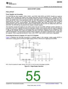
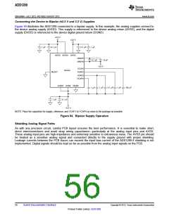
Connecting the Device to Bipolar (±2.5 V and 3.3 V) Supplies
Figure 54 illustrates the ADS1299 connected to a bipolar supply. In this example, the analog supplies connect to
the device analog supply (AVDD). This supply is referenced to the device analog return (AVSS), and the digital
supply (DVDD) is referenced to the device digital ground return (DGND).
+2.5 V
+3.3 V
1 mF
0.1 mF
0.1 mF
1 mF
AVDD AVDD1 DVDD
VREFP
0.1 mF
10 mF
VREFN
-2.5 V
VCAP1
VCAP2
VCAP3
VCAP4
Device
RESV1
AVSS1 AVSS DGND
1 mF
0.1 mF
1 mF
100 mF
1 mF
1 mF
0.1 mF
-2.5 V
NOTE: Place the capacitors for supply, reference, and VCAP1 to VCAP4 as close to the package as possible.
Figure 54. Bipolar Supply Operation
Shielding Analog Signal Paths
As with any precision circuit, careful PCB layout ensures the best performance. It is essential to make short,
direct interconnections and avoid stray wiring capacitance—particularly at the analog input pins and AVSS.
These analog input pins are high-impedance and extremely sensitive to extraneous noise. The AVSS pin should
be treated as a sensitive analog signal and connected directly to the supply ground with proper shielding.
Leakage currents between the PCB traces can exceed the input bias current of the ADS1299 if shielding is not
implemented. Digital signals should be kept as far as possible from the analog input signals on the PCB.
56
Submit Documentation Feedback
Copyright © 2012, Texas Instruments Incorporated
Product Folder Link(s): ADS1299

 TI [ TEXAS INSTRUMENTS ]