ADS1299
SBAS499A –JULY 2012–REVISED AUGUST 2012
www.ti.com
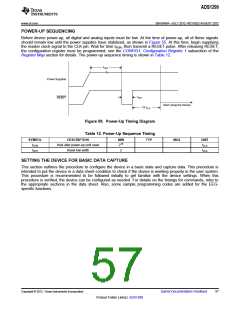
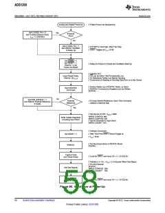
Analog and Digital Power-Up
// Follow Power-Up Sequencing
Set CLKSEL Pin = 0
and Provide External Clock
fCLK = 2.048 MHz
Yes
External
Clock
No
Set CLKSEL Pin = 1
and Wait for Oscillator
to Wake Up
// If START is Tied High, After This Step
// DRDY Toggles at fCLK / 8192
Set PDWN = 1
Set RESET = 1
Wait for 1 s for
Power-On Reset
// Delay for Power-On Reset and Oscillator Start-Up
// Activate DUT
// CS can be Either Tied Permanently Low
// Or Selectively Pulled Low Before Sending
// Commands or Reading or Sending Data from or to the Device
Issue Reset Pulse,
s
Wait for 18 tCLK
// Device Wakes Up in RDATAC Mode, so Send
// SDATAC Command so Registers can be Written
SDATAC
Send SDATAC
Command
No
Set PDB_REFBUF = 1
and Wait for Internal Reference
to Settle
External
Reference
// If Using Internal Reference, Send This Command
¾WREG CONFIG3 E0h
Yes
// Set Device for DR = fMOD / 4096
WREG CONFIG1 96h
Write Certain Registers,
Including Input Short
WREG CONFIG2 C0h
// Set All Channels to Input Short
WREG CHnSET 01h
// Activate Conversion
// After This Point DRDY Should Toggle at
// fCLK / 8192
Set START = 1
RDATAC
// Put the Device Back in RDATAC Mode
RDATAC
Capture Data
and Check Noise
// Look for DRDY and Issue 24 + n ´ 24 SCLKs
// Activate a (1 mV ´ VREF / 2.4) Square-Wave Test Signal
// On All Channels
SDATAC
WREG CONFIG2 D0h
WREG CHnSET 05h
RDATAC
Set Test Signals
Capture Data
and Test Signal
// Look for DRDY and Issue 24 + n ´ 24 SCLKs
Figure 56. Initial Flow at Power-Up
58
Submit Documentation Feedback
Copyright © 2012, Texas Instruments Incorporated
Product Folder Link(s): ADS1299

 TI [ TEXAS INSTRUMENTS ]