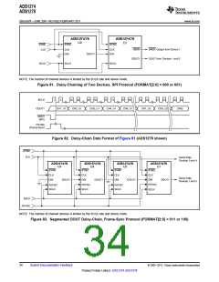
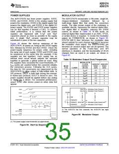
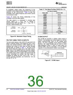
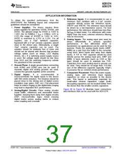
ADS1274
ADS1278
SBAS367F –JUNE 2007–REVISED FEBRUARY 2011
www.ti.com
THS4521(1)
+3.3V
ADS1274/ADS1278
TMS320VC5509
IN1(+)
AINP1
IOVDD
DVDD (I/O)
10mF(2)
IN1(-)
AINN1
2.2nF(3)
CLK
DRDY/FSYNC
DOUT1
50W
FSR
DR
U2
0
Q
U1
CVDD
(CORE)
>
+1.6V
SCLK
Q
50W
DOUT2
CLKR
See
Note (5)
200MHz
DOUT3
IN4/8(+)
AINP4/8
AINN4/8
DOUT4
IN4/8(-)
2.2nF(3)
+5V
SYNC
PWDN1
PWDN2
PWDN3
PWDN4
I/O
AVDD
DVDD
+
10mF(2)
+1.8V(6)
10mF(2)
See
Note (6)
1mF
REF5025
VREFP
VREFN
+
10mF
0.1mF(2)
+3.3V
CLKDIV
(High-Speed, Frame-Sync, TDM,
and Fixed-Position data selected.)
MODE0
MODE1
VCOM
+5V
0.1mF(2)
(4)
TEST0
TEST1
DIN
+3.3V
FORMAT2
FORMAT1
100W
Buffered
VCOM
Output
OPA350
AGND
DGND
FORMAT0
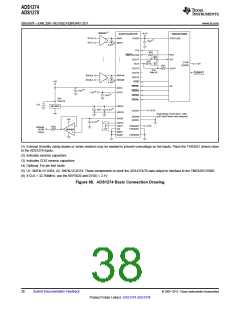
(1) External Schottky clamp diodes or series resistors may be needed to prevent overvoltage on the inputs. Place the THS4521 drivers close
to the ADS1278 inputs.
(2) Indicates ceramic capacitors.
(3) Indicates COG ceramic capacitors.
(4) Optional. For pin test mode.
(5) U1: SN74LVC1G04; U2: SN74LVC2G74. These components re-clock the ADS1274/78 data output to interface to the TMS320VC5509.
(6) If CLK > 32.768MHz, use the REF5020 and DVDD = 2.1V.
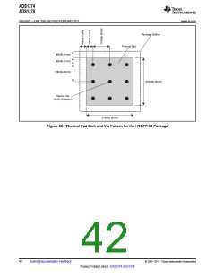
Figure 88. ADS1274 Basic Connection Drawing
38
Submit Documentation Feedback
© 2007–2011, Texas Instruments Incorporated
Product Folder Link(s): ADS1274 ADS1278

 TI [ TEXAS INSTRUMENTS ]