ADS1274
ADS1278
SBAS367F –JUNE 2007–REVISED FEBRUARY 2011
www.ti.com
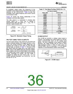
Table 17. Test Mode Pin Map (TEST[1:0] = 11)
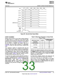
In modulator output mode, the frequency of the
modulator clock output (SCLK) depends on the mode
selection of the ADS1274/78. Table 16 lists the
modulator clock output frequency and DVDD current
versus device mode.
TEST MODE PIN MAP
INPUT PINS
OUTPUT PINS
DOUT1
DOUT2
DOUT3
DOUT4
DOUT5
DOUT6
DOUT7
DOUT8
DIN
PWDN1
PWDN2
PWDN3
PWDN4
PWDN5
PWDN6
PWDN7
PWDN8
MODE0
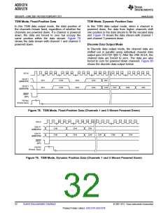
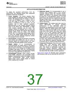
Figure 86 shows the timing relationship of the
modulator clock and data outputs.
The data output is a modulated 1s density data
stream. When VIN = +VREF, the 1s density is
approximately 80% and when VIN = –VREF, the 1s
density is approximately 20%.
Modulator
SCLK
Clock Output
MODE1
SYNC
FORMAT0
FORMAT1
FORMAT2
CLKDIV
FSYNC/DRDY
SCLK
Modulator
DOUT
Data Output
(13ns max)
Figure 86. Modulator Output Timing
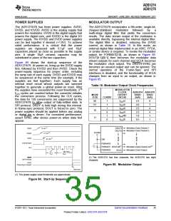
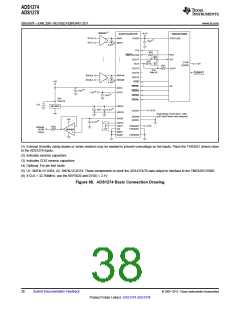
VCOM OUTPUT
The VCOM pin provides a voltage output equal to
AVDD/2. The intended use of this output is to set the
output common-mode level of the analog input
drivers. The drive capability of the output is limited;
therefore, the output should only be used to drive
high-impedance nodes (> 1MΩ). In some cases, an
external buffer may be necessary. A 0.1μF bypass
capacitor is recommended to reduce noise pickup.
PIN TEST USING TEST[1:0] INPUTS
The test mode feature of the ADS1274 and ADS1278
allows continuity testing of the digital I/O pins. In this
mode, the normal functions of the digital pins are
disabled and routed to each other as pairs through
internal logic, as shown in Table 17. The pins in the
left column drive the output pins in the right column.
Note: some of the digital input pins become outputs;
these outputs must be accommodated in the design.
The analog input, power supply, and ground pins all
remain connected as normal. The test mode is
engaged by setting the pins TEST [1:0] = 11. For
normal converter operation, set TEST[1:0] = 00. Do
not use '01' or '10'.
ADS1274/78
OPA350
VCOM » (AVDD/2)
0.1mF
Figure 87. VCOM Output
36
Submit Documentation Feedback
© 2007–2011, Texas Instruments Incorporated
Product Folder Link(s): ADS1274 ADS1278

 TI [ TEXAS INSTRUMENTS ]