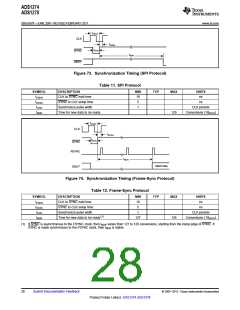
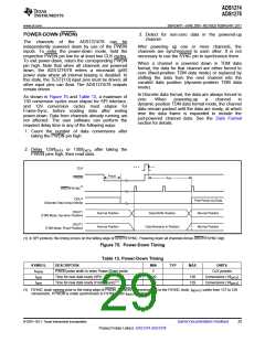
ADS1274
ADS1278
SBAS367F –JUNE 2007–REVISED FEBRUARY 2011
www.ti.com
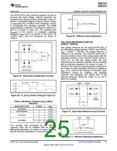
ESD diodes protect the reference inputs. To keep
these diodes from turning on, make sure the voltages
on the reference pins do not go below AGND by
more than 0.4V, and likewise do not exceed AVDD by
0.4V. If these conditions are possible, external
Schottky clamp diodes or series resistors may be
required to limit the input current to safe values (see
the Absolute Maximum Ratings table).
As with any high-speed data converter, a high-quality,
low-jitter clock is essential for optimum performance.
Crystal clock oscillators are the recommended clock
source. Make sure to avoid excess ringing on the
clock input; keeping the clock trace as short as
possible, and using a 50Ω series resistor placed
close to the source end, often helps.
Table 8. Clock Input Options
A high-quality reference voltage with the appropriate
drive strength is essential for achieving the best
performance from the ADS1274. Noise and drift on
the reference degrade overall system performance.
See the Application Information section for example
reference circuits.
MODE
SELECTION
MAX fCLK
(MHz)
DATA RATE
(SPS)
CLKDIV fCLK/fDATA
High-Speed
37
27
1
1
1
0
1
0
256
512
144,531
52,734
High-Resolution
27
512
Low-Power
Low-Speed
52,734
10,547
13.5
27
256
CLOCK INPUT (CLK)
2,560
512
5.4
The ADS1274/78 requires a clock input for operation.
The individual converters of the ADS1274/78 operate
from the same clock input. At the maximum data rate,
the clock input can be either 27MHz or 13.5MHz for
Low-Power mode, or 27MHz or 5.4MHz for
Low-Speed mode, determined by the setting of the
CLKDIV input. For High-Speed mode, the maximum
CLK input frequency is 37MHz. For High-Resolution
mode, the maximum CLK input frequency is 27MHz.
In High-Speed mode, operating conditions are
restricted depending on the clock input frequency.
The limitations are summarized in Table 7.
MODE SELECTION (MODE)
The ADS1274/78 supports four modes of operation:
High-Speed, High-Resolution, Low-Power, and
Low-Speed. The modes offer optimization of speed,
resolution, and power. Mode selection is determined
by the status of the digital input MODE[1:0] pins, as
shown in Table 9. The ADS1274/78 continually
monitors the status of the MODE pin during
operation.
Table 9. Mode Selection
Table 7. High-Speed Mode fCLK Conditions
(1)
MODE[1:0]
MODE SELECTION
High-Speed
MAX fDATA
144,531
52,734
VREF
00
01
10
11
fCLK (MHz)
(V)
DVDD (V)
INTERFACE
High-Resolution
Low-Power
0.5 to
3.1
0.1 ≤ fCLK ≤ 27
1.65 to 1.95 Frame-Sync or SPI
52,734
0.5 to
2.6
Low-Speed
10,547
27 < fCLK ≤ 32.768
32.768 < fCLK ≤ 37
1.65 to 1.95
2.0 to 2.2
Frame-Sync
Frame-Sync
(1) fCLK = 27MHz max (37MHz max in High-Speed mode).
0.5 to
2.1
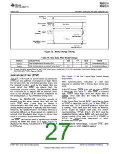
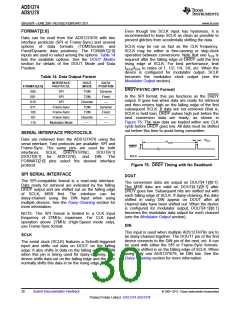
When using the SPI protocol, DRDY is held high after
a mode change occurs until settled (or valid) data are
ready; see Figure 72 and Table 10.
The selection of the external clock frequency (fCLK
does not affect the resolution of the ADS1274/78.
Use of slower fCLK can reduce the power
consumption of an external clock buffer. The output
data rate scales with clock frequency, down to a
minimum clock frequency of fCLK = 100kHz. Table 8
summarizes the ratio of the clock input frequency
(fCLK) to data rate (fDATA), maximum data rate and
corresponding maximum clock input for the four
operating modes.
)
In Frame-Sync protocol, the DOUT pins are held low
after a mode change occurs until settled data are
ready; see Figure 72 and Table 10. Data can be read
from the device to detect when DOUT changes to
logic 1, indicating that the data are valid.
a
26
Submit Documentation Feedback
© 2007–2011, Texas Instruments Incorporated
Product Folder Link(s): ADS1274 ADS1278

 TI [ TEXAS INSTRUMENTS ]