ADS1274
ADS1278
SBAS367F –JUNE 2007–REVISED FEBRUARY 2011
www.ti.com
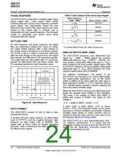
Table 5. Ideal Output Code versus Input Signal
PHASE RESPONSE
INPUT SIGNAL VIN
(AINP – AINN)
The ADS1274/78 incorporates a multiple stage, linear
phase digital filter. Linear phase filters exhibit
constant delay time versus input frequency (constant
group delay). This characteristic means the time
delay from any instant of the input signal to the same
instant of the output data is constant and is
independent of input signal frequency. This behavior
results in essentially zero phase errors when
analyzing multi-tone signals.
IDEAL OUTPUT CODE(1)
≥ +VREF
7FFFFFh
) VREF
223 * 1
0
000001h
000000h
FFFFFFh
* VREF
223 * 1
223
REFǒ * 1Ǔ
v −V
800000h
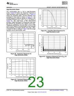
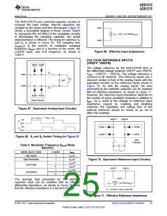
SETTLING TIME
223
As with frequency and phase response, the digital
filter also determines settling time. Figure 66 shows
the output settling behavior after a step change on
the analog inputs normalized to conversion periods.
The X-axis is given in units of conversion. Note that
after the step change on the input occurs, the output
data change very little prior to 30 conversion periods.
The output data are fully settled after 76 conversion
periods for High-Speed and Low-Power modes, and
78 conversion periods for High-Resolution mode.
(1) Excludes effects of noise, INL, offset, and gain errors.
ANALOG INPUTS (AINP, AINN)
The ADS1274/78 measures each differential input
signal VIN = (AINP – AINN) against the common
differential reference VREF = (VREFP – VREFN). The
most positive measurable differential input is +VREF
,
which produces the most positive digital output code
of 7FFFFFh. Likewise, the most negative measurable
differential input is –VREF, which produces the most
negative digital output code of 800000h.
Final Value
100
For optimum performance, the inputs of the
ADS1274/78 are intended to be driven differentially.
For single-ended applications, one of the inputs
(AINP or AINN) can be driven while the other input is
fixed (typically to AGND or +2.5V). Fixing the input to
2.5V permits bipolar operation, thereby allowing full
use of the entire converter range.
Fully Settled Data
at 76 Conversions
(78 Conversions for
High-Resolution mode)
Initial Value
0
While the ADS1274/78 measures the differential input
signal, the absolute input voltage is also important.
This value is the voltage on either input (AINP or
AINN) with respect to AGND. The range for this
voltage is:
0
10
20
30
40
50
60
70
80
Conversions (1/fDATA
)
Figure 66. Step Response
–0.1V < (AINN or AINP) < AVDD + 0.1V
If either input is taken below –0.4V or above
(AVDD + 0.4V), ESD protection diodes on the inputs
may turn on. If these conditions are possible, external
Schottky clamp diodes or series resistors may be
required to limit the input current to safe values (see
the Absolute Maximum Ratings table).
DATA FORMAT
The ADS1274/78 outputs 24 bits of data in twos
complement format.
A positive full-scale input produces an ideal output
code of 7FFFFFh, and the negative full-scale input
produces an ideal output code of 800000h. The
output clips at these codes for signals exceeding
full-scale. Table 5 summarizes the ideal output codes
for different input signals.
The ADS1274/78 is a very high-performance ADC.
For optimum performance, it is critical that the
appropriate circuitry be used to drive the ADS1274/78
inputs. See the Application Information section for
several recommended circuits.
24
Submit Documentation Feedback
© 2007–2011, Texas Instruments Incorporated
Product Folder Link(s): ADS1274 ADS1278

 TI [ TEXAS INSTRUMENTS ]