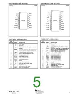
PIN CONFIGURATION (ADS1242)
PIN CONFIGURATION (ADS1243)
Top View
TSSOP
Top View
TSSOP
VDD
XIN
1
2
3
4
5
6
7
8
9
20 DRDY
19 SCLK
18 DOUT
17 DIN
VDD
XIN
1
2
3
4
5
6
7
8
16 DRDY
15 SCLK
14 DOUT
13 DIN
XOUT
XOUT
PDWN
VREF+
VREF–
AIN0/D0
PDWN
VREF+
VREF–
AIN0/D0
16 CS
ADS1243
ADS1242
12 CS
15 GND
11 GND
14
13
12
11
AIN3/D3
AIN2/D2
AIN7/D7
AIN6/D6
10
9
A
IN3/D3
IN2/D2
A
A
A
IN1/D1
A
IN1/D1
A
IN4/D4
IN5/D5 10
PIN DESCRIPTIONS (ADS1243)
PIN DESCRIPTIONS (ADS1242)
PIN
PIN
NUMBER
NAME
DESCRIPTION
NUMBER
NAME
DESCRIPTION
1
2
3
VDD
XIN
Power Supply
Clock Input
1
2
3
VDD
XIN
Power Supply
Clock Input
XOUT
Clock Output, used with crystal or ceramic
resonator.
XOUT
Clock Output, used with crystal or ceramic
resonator.
4
PDWN
Active LOW. Power Down. The power down func-
tion shuts down the analog and digital circuits.
Positive Differential Reference Input
Negative Differential Reference Input
Analog Input 0/Data I/O 0
Analog Input 1/Data I/O 1
Analog Input 4/Data I/O 4
Analog Input 5/Data I/O 5
Analog Input 6/Data I/O 6
Analog Input 7/Data I/O 7
Analog Input 2/Data I/O 2
Analog Input 3/Data I/O 3
Ground
4
PDWN
Active LOW. Power Down. The power down func-
tion shuts down the analog and digital circuits.
5
6
7
8
VREF+
VREF–
AIN0/D0
AIN1/D1
5
6
VREF+
VREF–
Positive Differential Reference Input
Negative Differential Reference Input
Analog Input 0/Data I/O 0
Analog Input 1/Data I/O 1
Analog Input 2/Data I/O 2
Analog Input 3/Data I/O 3
Ground
7
A
IN0/D0
IN1/D1
IN2/D2
IN3/D3
GND
CS
9
AIN4/D4
10
11
12
13
14
15
16
17
18
19
20
AIN5/D5
AIN6/D6
AIN7/D7
AIN2/D2
AIN3/D3
GND
CS
DIN
DOUT
SCLK
DRDY
8
A
A
A
9
10
11
12
13
14
15
16
Active LOW, Chip Select
Serial Data Input, Schmitt Trigger
Serial Data Output
Active LOW, Chip Select
Serial Data Input, Schmitt Trigger
Serial Data Output
Serial Clock, Schmitt Trigger
Active LOW, Data Ready
DIN
DOUT
SCLK
DRDY
Serial Clock, Schmitt Trigger
Active LOW, Data Ready
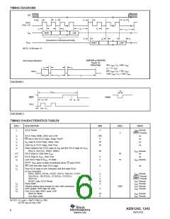
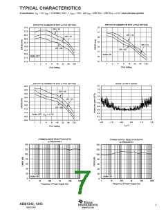
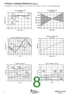
ADS1242, 1243
5
SBAS235B
www.ti.com

 TI [ TEXAS INSTRUMENTS ]