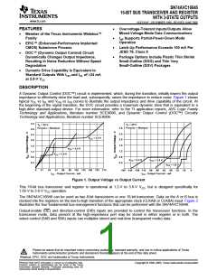
SN74AVC16646
16-BIT BUS TRANSCEIVER AND REGISTER
WITH 3-STATE OUTPUTS
www.ti.com
SCES181F–DECEMBER 1998–REVISED JUNE 2005
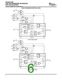
DESCRIPTION (CONTINUED)
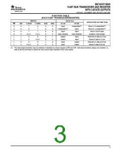
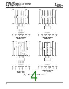
The circuitry used for select control eliminates the typical decoding glitch that occurs in a multiplexer during the
transition between stored and real-time data. DIR determines which bus receives data when OE is low. In the
isolation mode (OE high), A data may be stored in one register and/or B data may be stored in the other register.
When an output function is disabled, the input function still is enabled and may be used to store and transmit
data. Only one of the two buses, A or B, can be driven at a time.
To ensure the high-impedance state during power up or power down, OE should be tied to VCC through a pullup
resistor; the minimum value of the resistor is determined by the current-sinking capability of the driver.
This device is fully specified for partial-power-down applications using Ioff. The Ioff circuitry disables the outputs,
preventing damaging current backflow through the device when it is powered down.
The SN74AVC16646 is characterized for operation from –40°C to 85°C.
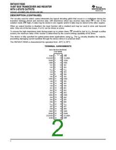
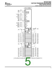
TERMINAL ASSIGNMENTS
DGG OR DGV PACKAGE
(TOP VIEW)
1
56
55
54
53
52
51
50
49
48
47
46
45
44
43
42
41
40
39
38
37
36
35
34
33
32
31
30
29
1DIR
1CLKAB
1SAB
GND
1OE
2
1CLKBA
1SBA
GND
1B1
3
4
5
1A1
1A2
6
1B2
7
V
CC
V
CC
8
1A3
1A4
1A5
GND
1A6
1A7
1A8
2A1
2A2
2A3
GND
2A4
2A5
2A6
1B3
1B4
1B5
GND
1B6
1B7
1B8
2B1
2B2
2B3
GND
2B4
2B5
2B6
9
10
11
12
13
14
15
16
17
18
19
20
21
22
23
24
25
26
27
28
V
CC
V
CC
2A7
2A8
2B7
2B8
GND
GND
2SBA
2CLKBA
2OE
2SAB
2CLKAB
2DIR
2

 TI [ TEXAS INSTRUMENTS ]