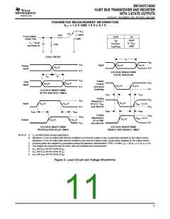
SN74AVC16646
16-BIT BUS TRANSCEIVER AND REGISTER
WITH 3-STATE OUTPUTS
www.ti.com
SCES181F–DECEMBER 1998–REVISED JUNE 2005
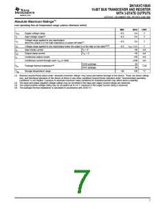
Absolute Maximum Ratings(1)
over operating free-air temperature range (unless otherwise noted)
MIN
–0.5
–0.5
MAX
4.6
UNIT
V
VCC
VI
Supply voltage range
Input voltage range(2)
4.6
V
Voltage range applied to any input/output
VO
–0.5
–0.5
4.6
V
when the output is in the high-impedance or power-off state(2)
VO
IIK
Voltage range applied to any input/output when the output is in the high or low state(2)(3)
VCC + 0.5
–50
V
Input clamp current
VI < 0
mA
mA
mA
mA
IOK
IO
Output clamp current
VO < 0
–50
Continuous output current
Continuous current through each VCC or GND
±50
±100
64
DGG package
DGV package
θJA
Package thermal impedance(4)
Storage temperature range
°C/W
°C
48
Tstg
–65
150
(1) Stresses beyond those listed under "absolute maximum ratings" may cause permanent damage to the device. These are stress ratings
only, and functional operation of the device at these or any other conditions beyond those indicated under "recommended operating
conditions" is not implied. Exposure to absolute-maximum-rated conditions for extended periods may affect device reliability.
(2) The input and output negative-voltage ratings may be exceeded if the input and output current ratings are observed.
(3) The output positive-voltage rating may be exceeded up to 4.6 V maximum if the output current rating is observed.
(4) The package thermal impedance is calculated in accordance with JESD 51.
7

 TI [ TEXAS INSTRUMENTS ]