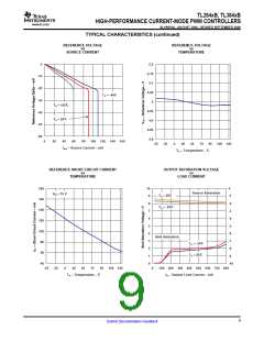
TL284xB, TL384xB
HIGH-PERFORMANCE CURRENT-MODE PWM CONTROLLERS
www.ti.com
SLVS610A–AUGUST 2006–REVISED SEPTEMBER 2006
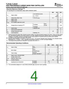
Absolute Maximum Ratings(1)(2)
over operating free-air temperature range (unless otherwise noted)
MIN
MAX
UNIT
Low impedance source
30
VCC
Supply voltage
V
Self
limiting
ICC < 30 mA
VI
Analog input voltage range
Supply current
VFB and ISENSE
–0.3
6.3
30
V
mA
A
ICC
IO
Output current
±1
IO(sink)
Error amplifier output sink current
10
mA
8 pin
97
D package
θJA
Package thermal impedance(3)(4)
14 pin
86
°C/W
P package
85
Output energy
Capacitive load
5
µJ
°C
°C
°C
TJ
Virtual junction temperature
Storage temperature range
Lead temperature
150
150
300
Tstg
Tlead
–65
Soldering, 10 s
(1) Stresses beyond those listed under "absolute maximum ratings" may cause permanent damage to the device. These are stress ratings
only, and functional operation of the device at these or any other conditions beyond those indicated under "recommended operating
conditions" is not implied. Exposure to absolute-maximum-rated conditions for extended periods may affect device reliability.
(2) All voltages are with respect to the device GND terminal.
(3) Maximum power dissipation is a function of TJ(max), θJA, and TA. The maximum allowable power dissipation at any allowable ambient
temperature is PD = (TJ(max) – TA)/θJA. Operating at the absolute maximum TJ of 150°C can impact reliability.
(4) The package thermal impedance is calculated in accordance with JESD 51-7.
Recommended Operating Conditions
MIN
NOM
MAX
30
UNIT
VCC
VC(1)
VCC
Supply voltage
Input voltage
Output voltage
V
30
RT/CT
0
0
5.5
5.5
30
VI
V
V
VFB and ISENSE
OUTPUT
POWER GROUND(1)
0
VO
–0.1
1
ICC
IO
IO(ref)
fosc
Supply current, externally limited
Average output current
Reference output current
Oscillator frequency
25
mA
mA
mA
kHz
200
–20
500
85
100
TL284xB
TL384xB
–40
0
TJ
Operating free-air temperature
°C
70
(1) The recommended voltages for VC and POWER GROUND apply only to the 14-pin D package.
4
Submit Documentation Feedback

 TI [ TEXAS INSTRUMENTS ]