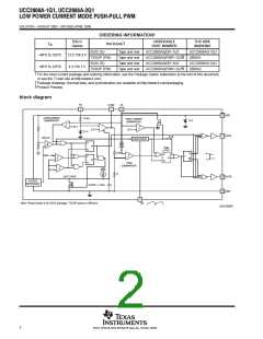
ꢀ ꢁꢁꢂ ꢃ ꢄ ꢃ ꢅꢆꢇ ꢈꢇꢉ ꢀꢁ ꢁꢂ ꢃ ꢄ ꢃ ꢅꢆꢂ ꢈꢇ
ꢋ
ꢊ
ꢋ
ꢌ
ꢍ
ꢋ
ꢌ
ꢎ
ꢏ
ꢁ
ꢀ
ꢏ
ꢏ
ꢎ
ꢐ
ꢑ
ꢒ
ꢓ
ꢎ
ꢍ
ꢀ
ꢔ
ꢕ
ꢆ
ꢍ
ꢀ
ꢊꢊ
ꢍ
ꢌ
ꢒ
SGLS183A − AUGUST 2003 − REVISED APRIL 2008
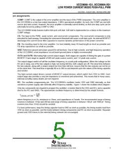
pin assignments (continued)
RC
4
1.41
RC
FREQUENCY =
VDD
2
(APPROXIMATE
FREQUENCY)
S
R
Q
OSCILLATOR
OUTPUT
0.2 V
UDG-00095
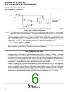
Figure 1. Block Diagram for Oscillator
NOTE A: The oscillator generates a sawtooth waveform on RC. During the RC rise time, the output stages alternate on time, but both stages are
off during the RC fall time. The output stages switch a 1/2 the oscillator frequency, with ensured duty cycle of < 50% for both outputs.
VDD: The power input connection for this device. Although quiescent VDD current is very low, total supply
current will be higher, depending on OUTA and OUTB current, and the programmed oscillator frequency. Total
VDD current is the sum of quiescent VDD current and the average OUT current. Knowing the operating
frequency and the MOSFET gate charge (Qg), average OUT current can be calculated from:
I
+ Q F, where F is frequency
g
OUT
To prevent noise problems, bypass VDD to GND with a ceramic capacitor as close to the chip as possible along
with an electrolytic capacitor. A 1-µF decoupling capacitor is recommended.
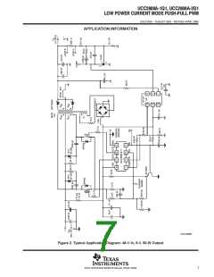
APPLICATION INFORMATION
A 200-kHz push-pull application circuit with a full-wave rectifier is shown in Figure 2. The output, V , provides
O
5 V at 50 W maximum and is electrically isolated from the input. Since the UCC2808A is a peak-current-mode
controller the 2N2907 emitter following amplifier (buffers the CT waveform) provides slope compensation which
is necessary for duty ratios greater than 50%. Capacitor decoupling is very important with a single ground IC
controller, and a 1 µF is suggested as close to the IC as possible. The controller supply is a series RC for start-up,
paralleled with a bias winding on the output inductor used in steady state operation.
Isolation is provided by an optocoupler with regulation done on the secondary side using the TL431 adjustable
precision shunt regulator. Small signal compensation with tight voltage regulation is achieved using this part
on the secondary side. Many choices exist for the output inductor depending on cost, volume, and mechanicall
strength. Several design options are iron powder, molypermalloy (MPP), or a ferrite core with an air gap as
shown here. The main power transformer has a Magnetics Inc. ER28 size core made of P material for efficient
operation at this frequency and temperature. The input voltage may range from 36 V dc to 72 V dc.
6
POST OFFICE BOX 655303 • DALLAS, TEXAS 75265

 TI [ TEXAS INSTRUMENTS ]