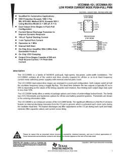
ꢀꢁꢁ ꢂ ꢃꢄ ꢃ ꢅ ꢆꢇꢈ ꢇ ꢉ ꢀꢁꢁ ꢂ ꢃꢄ ꢃꢅ ꢆꢂ ꢈ ꢇ
ꢊ ꢋ ꢌ ꢍꢋ ꢌ ꢎꢏ ꢁꢀꢏ ꢏꢎꢐꢑ ꢒ ꢋꢓ ꢎ ꢍꢀꢔ ꢕꢆꢍ ꢀꢊ ꢊ ꢍ ꢌꢒ
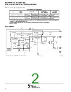
SGLS183A − AUGUST 2003 − REVISED APRIL 2008
†}
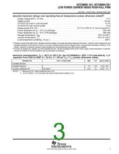
absolute maximum ratings over operating free-air temperature (unless otherwise noted)
Supply voltage (IDD ≤ 10 mA) . . . . . . . . . . . . . . . . . . . . . . . . . . . . . . . . . . . . . . . . . . . . . . . . . . . . . . . . . . . . . . . 15 V
Supply current . . . . . . . . . . . . . . . . . . . . . . . . . . . . . . . . . . . . . . . . . . . . . . . . . . . . . . . . . . . . . . . . . . . . . . . . . . . 20 mA
OUTA/OUTB source current (peak) . . . . . . . . . . . . . . . . . . . . . . . . . . . . . . . . . . . . . . . . . . . . . . . . . . . . . . . . . −0.5 A
OUTA/OUTB sink current (peak) . . . . . . . . . . . . . . . . . . . . . . . . . . . . . . . . . . . . . . . . . . . . . . . . . . . . . . . . . . . . 1.0 A
Analog inputs (FB, CS) . . . . . . . . . . . . . . . . . . . . . . . . . . . . . . . . . . . . . . −0.3 V to VDD 0.3 V, not to exceed 6 V
Power dissipation at T = 25°C (D package) . . . . . . . . . . . . . . . . . . . . . . . . . . . . . . . . . . . . . . . . . . . . . . . . 650 mW
A
Power dissipation at T = 25°C (PW package) . . . . . . . . . . . . . . . . . . . . . . . . . . . . . . . . . . . . . . . . . . . . . . 400 mW
A
stg
Storage temperature, T
. . . . . . . . . . . . . . . . . . . . . . . . . . . . . . . . . . . . . . . . . . . . . . . . . . . . . . . . . . −65°C to150°C
Junction temperature, T . . . . . . . . . . . . . . . . . . . . . . . . . . . . . . . . . . . . . . . . . . . . . . . . . . . . . . . . . . −55°C to 150°C
Lead temperature (soldering, 10 sec.) . . . . . . . . . . . . . . . . . . . . . . . . . . . . . . . . . . . . . . . . . . . . . . . . . . . . . . 300°C
J
†
†
Stresses beyond those listed under “absolute maximum ratings” may cause permanent damage to the device. These are stress ratings only, and
functional operation of the device at these or any other conditions beyond those indicated under “recommended operating conditions” is not
implied. Exposure to absolute-maximum-rated conditions for extended periods may affect device reliability.
Currents are positive into, negative out of the specified terminal. Consult Packaging Section of the Power Supply Control Data Book (TI Literature
Number SLUD003) for thermal limitations and considerations of packages.
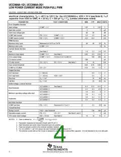
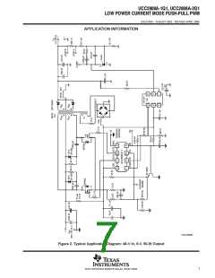
electrical characteristics, T = −40°C to 125°C for the UCC2808AQ-x, VDD = 10 V (see Note 6), 1-µF
A
capacitor from VDD to GND, R = 22 kΩ, C = 330 pF T = T , (unless otherwise noted)
A
J
PARAMETER
TEST CONDITIONS
MIN
TYP
MAX UNITS
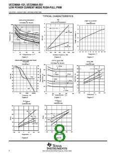
Oscillator Section
Oscillator frequency
175
194
0.5
213
kHz
V/V
Oscillator amplitude/VDD
See Note 1
0.44
0.56
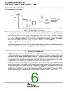
NOTES: 1. Measured at RC. Signal amplitude tracks VDD.
6. For UCCx808A−1, set VDD above the start threshold before setting at 10 V.
3
POST OFFICE BOX 655303 • DALLAS, TEXAS 75265

 TI [ TEXAS INSTRUMENTS ]