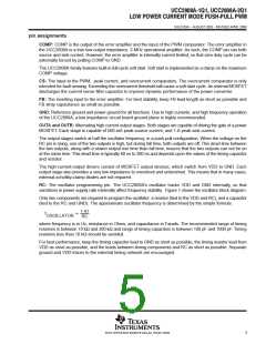
ꢀ ꢁꢁꢂ ꢃ ꢄ ꢃ ꢅꢆꢇ ꢈꢇꢉ ꢀꢁ ꢁꢂ ꢃ ꢄ ꢃ ꢅꢆꢂ ꢈꢇ
ꢊ ꢋꢌ ꢍꢋꢌ ꢎꢏ ꢁ ꢀꢏ ꢏꢎ ꢐꢑ ꢒꢋ ꢓꢎ ꢍ ꢀꢔ ꢕꢆꢍꢀ ꢊꢊ ꢍꢌ ꢒ
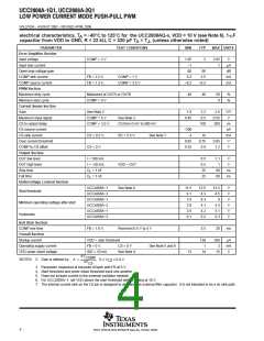
SGLS183A − AUGUST 2003 − REVISED APRIL 2008
electrical characteristics, T = −40°C to 125°C for the UCC2808AQ-x, VDD = 10 V (see Note 6), 1-µF
A
capacitor from VDD to GND, R = 22 kΩ, C = 330 pF T = T , (unless otherwise noted)
A
J
PARAMETER
TEST CONDITIONS
MIN
TYP
MAX UNITS
Error Amplifier Section
Input voltage
COMP = 2 V
1.95
–1
2
2.05
1
V
Input bias current
Open loop voltage gain
COMP sink current
COMP source current
PWM Section
µA
dB
mA
mA
60
80
2.5
FB = 2.2 V,
FB = 1.3 V,
COMP = 1 V
0.3
–0.2
COMP = 3.5 V
–0.5
Maximum duty cycle
Minimum duty cycle
Current Sense Section
Gain
Measured at OUTA or OUTB
COMP = 0 V
48
49
50
0
%
%
See Note 2
1.9
2.2
0.5
2.5
0.55
200
V/V
V
Maximum input signal
CS to output delay
CS source current
CS sink current
COMP = 5 V
See Note 3
CS from 0 mV to 600 mV
0.45
COMP = 3.5 V,
100
ns
nA
mA
V
−200
4
CS = 0.5 V,
CS = 0 V
RC = 5.5 V
See Note 7
10
0.75
0.8
Over current threshold
COMP to CS offset
Output Section
OUT low level
0.65
0.35
0.85
1.2
V
I = 100 mA
I = −50 mA,
0.5
0.5
25
1.1
1
V
V
OUT high level
VDD – OUT
See Note 6
Rise time
C
C
= 1 nF
= 1 nF
60
60
ns
ns
L
L
Fall time
25
Undervoltage Lockout Section
UCCx808A−1
UCCx808A−2
UCCx808A−1
UCCx808A−2
UCCx808A−1
UCCx808A−2
11.5
4.1
7.6
3.9
3.5
0.1
12.5
4.3
8.3
4.1
4.2
0.2
13.5
4.5
9
V
V
V
V
V
V
Start threshold
Minimum operating voltage after start
Hysteresis
4.3
5.1
0.3
Soft Start Section
COMP rise time
FB = 1.8 V,
Rise from 0.5 V to 4 V
3.5
20
ms
Overall Section
Startup current
VDD < start threshold
130
1
260
2
µA
mA
V
Operating supply current
VDD zener shunt voltage
FB = 0 V,
IDD = 10 mA
COMP
CS = 0 V
See Note 4
See Note 5 and 6
13
14
15
DV
NOTES: 2. Gain is defined by: A +
,
0 ≤ V ≤ 0.4 V.
CS
DV
CS
3. Parameter measured at trip point of latch with FB at 0 V.
4. Start threshold and zener shunt threshold track one another.
5. Does not include current in the external oscillator network.
6. For UCC2808A−1, set VDD above the start threshold before setting at 10 V.
7. The internal current sink on the CS pin is designed to discharge an external filter capacitor. It is not intended to be a dc sink path.
4
POST OFFICE BOX 655303 • DALLAS, TEXAS 75265

 TI [ TEXAS INSTRUMENTS ]