ꢀꢁꢁ ꢂ ꢃꢄ ꢃ ꢅ ꢆꢇꢈ ꢇ ꢉ ꢀꢁꢁ ꢂ ꢃꢄ ꢃꢅ ꢆꢂ ꢈ ꢇ
ꢊ ꢋ ꢌ ꢍꢋ ꢌ ꢎꢏ ꢁꢀꢏ ꢏꢎꢐꢑ ꢒ ꢋꢓ ꢎ ꢍꢀꢔ ꢕꢆꢍ ꢀꢊ ꢊ ꢍ ꢌꢒ
SGLS183A − AUGUST 2003 − REVISED APRIL 2008
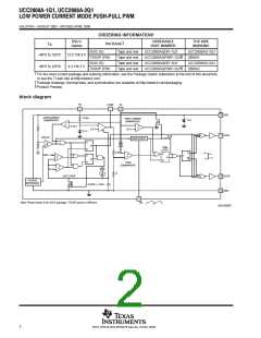
pin assignments
COMP: COMP is the output of the error amplifier and the input of the PWM comparator. The error amplifier in
the UCC2808A is a true low-output impedance, 2-MHz operational amplifier. As such, the COMP pin can both
source and sink current. However, the error amplifier is internally current limited, so that zero duty cycle can be
externally forced by pulling COMP to GND.
The UCC2808A family features built-in full-cycle soft start. Soft start is implemented as a clamp on the maximum
COMP voltage.
CS: The input to the PWM, peak current, and overcurrent comparators. The overcurrent comparator is only
intended for fault sensing. Exceeding the overcurrent threshold will cause a soft start cycle. An internal MOSFET
discharges the current sense filter capacitor to improve dynamic performance of the power converter.
FB: The inverting input to the error amplifier. For best stability, keep FB lead length as short as possible and
FB stray capacitance as small as possible.
GND: Reference ground and power ground for all functions. Due to high currents, and high frequency operation
of the UCC2808A, a low impedance circuit board ground plane is highly recommended.
OUTA and OUTB: Alternating high current output stages. Both stages are capable of driving the gate of a power
MOSFET. Each stage is capable of 500-mA peak-source current, and 1-A peak-sink current.
The output stages switch at half the oscillator frequency, in a push-pull configuration. When the voltage on the
RC pin is rising, one of the two outputs is high, but during fall time, both outputs are off. This dead time between
the two outputs, along with a slower output rise time than fall time, insures that the two outputs can not be on
at the same time. This dead time is typically 60 ns to 200 ns and depends upon the values of the timing capacitor
and resistor.
The high-current-output drivers consist of MOSFET output devices, which switch from VDD to GND. Each
output stage also provides a very low impedance to overshoot and undershoot. This means that in many cases,
external-schottky-clamp diodes are not required.
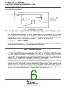
RC: The oscillator programming pin. The UCC2808A’s oscillator tracks VDD and GND internally, so that
variations in power supply rails minimally affect frequency stability. Figure 1 shows the oscillator block diagram.
Only two components are required to program the oscillator: a resistor (tied to the VDD and RC), and a capacitor
(tied to the RC and GND). The approximate oscillator frequency is determined by the simple formula:
1.41
RC
f
+
OSCILLATOR
where frequency is in Hz, resistance in Ohms, and capacitance in Farads. The recommended range of timing
resistors is between 10 kΩ and 200 kΩ and range of timing capacitors is between 100 pF and 1000 pF. Timing
resistors less than 10 kΩ should be avoided.
For best performance, keep the timing capacitor lead to GND as short as possible, the timing resistor lead from
VDD as short as possible, and the leads between timing components and RC as short as possible. Separate
ground and VDD traces to the external timing network are encouraged.
5
POST OFFICE BOX 655303 • DALLAS, TEXAS 75265

 TI [ TEXAS INSTRUMENTS ]