78Q8430 Data Sheet
DS_8430_001
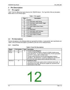
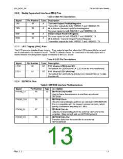
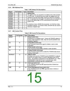
3 Pin Description
3.1 Pin Legend
Table 1 lists the different pin types found on the 78Q8430 device. The Type field of the pin description
tables refers to one of these types.
Table 1: Pin Legend
Type
A
Description
Analog
IU
IS
O
TTL-level Input, with Pull-up
TTL-level Input, with Schmitt Trigger
TTL-level Output
OD
S
TTL-level Output (Open Drain)
Supply
I
TTL-level Input
ID
B
TTL-level Input, with Pull-down
TTL-level Bidirectional Pin
TTL-level Output (Tristate)
Ground
OZ
G
3.2 Pin Descriptions
The pin descriptions in the following tables are grouped by interface. A pin number, type specification per
Table 2 and a functional description is provided for each pin on the 78Q8430 device.
3.2.1 Clock Pins
Table 2: Clock Pin Descriptions
Signal
XTLP
XTLN
Pin Number Type Description
87
88
A
Crystal Positive/Negative
To use the internal oscillator, connect a 25 MHz crystal across
XTLP and XTLN. To use of an external clock, XTLN is grounded
and XTLP is driven with a 25 MHz clock.
Provides timing reference for all media dependant interface
operations. An internal PLL is used to multiply this clock by four
for use as the main system clock in internal clock mode.
BUSCLK
15
I
Peripheral Clock
The source for the main system clock in external clock mode. In
synchronous bus mode, all host bus signals are assumed to be
synchronous to this clock.
12
Rev. 1.2

 TERIDIAN [ TERIDIAN SEMICONDUCTOR CORPORATION ]