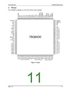
DS_8430_001
78Q8430 Data Sheet
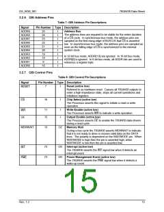
3.2.6 GBI Address Pins
Table 7: GBI Address Pin Descriptions
Signal
Pin Number Type Description
ADDR9
ADDR8
ADDR7
ADDR6
ADDR5
ADDR4
ADDR3
ADDR2
ADDR1
ADDR0
25
24
23
22
21
20
19
18
9
I
I
I
I
I
I
I
I
I
I
Address Bus
The address lines are required to be stable for the entire duration
of a CS cycle. In synchronous bus mode, the address pins are
sampled on the first rising edge of BUSCLK that CS is asserted
low. In asynchronous bus mode, the address pins are sampled as
soon as the falling edge of CS is synchronized to the internal
system clock.
In 32-bit bus mode, ADDR[1:0] are ignored. In 16-bit bus mode,
ADDR[0] is ignored. In 8-bit bus mode, all ADDR bits are used to
reference a register byte.
10
3.2.7 GBI Control Pins
Table 8: GBI Control Pin Descriptions
Signal
Pin Number Type Description
7
I
I
Reset (active low)
RESET
Referred to as hardware reset. Causes all 78Q8430 outputs to
enter a high-impedance state, stops all current operations and
initializes registers.
16
Chip Select (active low)
CS
The Processor asserts this signal to initiate a read or write
operation.
11
12
I
I
Write Enable (active low)
The Processor asserts WR to indicate a write operation.
WR
Output Enable (active low)
OE
The Processor asserts OE to enable the 78Q8430 data drivers
during a read cycle.
MEMWAIT
13
OZ
Memory Wait
During a bus cycle the 78Q8430 asserts MEMWAIT to indicate
that it is not ready to drive or receive valid data on the DATA
lines. The polarity is dependent on the WAITMODE pin. When
WAITMODE is high then the pin is asserted high; when
WAITMODE is low then the pin is asserted low.
72
73
OD
OD
Interrupt (active low)
The 78Q8430 asserts the INT signal low when it detects an
interrupt event.
INT
Power Management Event (active low)
The 78Q8430 asserts the PME signal low when it detects a
wake-up event.
PME
Rev. 1.2
15

 TERIDIAN [ TERIDIAN SEMICONDUCTOR CORPORATION ]