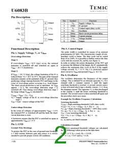
U6083B
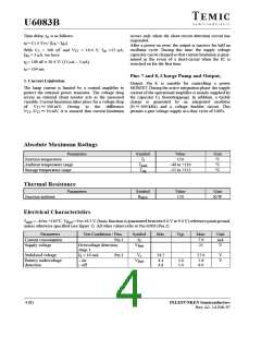
Time delay, t , is as follows:
occurs only when the short-circuit detection circuit has
responded.
d
t = C
V / (I – I )
T5 ch dis
d
5
After a power-on reset, the output is inactive for half an
oscillator cycle. During this time, the supply voltage
capacitor can be charged so that current limitation is guar-
anteed in the event of a short-circuit when the IC is
switched on for the first time.
With C = 100 nF and V = 10.4 V, I =13 A,
5
T5
ch
I
= 3 A, we have
dis
t = 100 nF 10.4 V/ (13 A – 3 A)
d
t = 104 ms
d
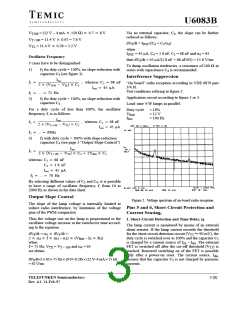
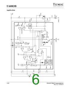
Pins 7 and 8, Charge Pump and Output,
2. Current Limitation:
Output, Pin 8, is suitable for controlling a power
The lamp current is limited by a control amplifier to MOSFET. During the active integration phase, the supply
protect the external power transistor. The voltage drop current of the operational amplifier is mainly supplied by
across an external shunt resistor acts as the measured the capacitor C (bootstrapping). In addition, a trickle
3
variable. Current limitation takes place for a voltage drop charge is generated by an integrated oscillator
of
V
–V
100 mV. Owing to the difference (f
10 mV, it is ensured that current limitation permits a gate voltage supply at a duty cycle of 100%.
400 kHz) and a voltage doubler circuit. This
T1
T2
7
V
T1
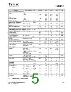
Absolute Maximum Ratings
Parameters
Junction temperature
Symbol
Value
150
Unit
°C
T
j
Ambient temperature range
Storage temperature range
T
T
–40 to +110
–55 to +125
°C
°C
amb
stg
Thermal Resistance
Parameters
Symbol
R
thJA
Value
120
Unit
K/W
Junction ambient
Electrical Characteristics
T
amb
= –40 to +110°C, V
= 9 to 16.5 V, (basic function is guaranteed between 6.0 V to 9.0 V) reference point ground,
Batt
unless otherwise specified (see figure 1). All other values refer to Pin GND (Pin 2).
Parameters
Current consumption
Supply voltage
Test Conditions / Pins
Pin 1
Overvoltage detection,
stage 1
Symbol
Min.
Typ.
Max.
7.9
25
Unit
mA
V
I
S
V
Batt
Stabilized voltage
Battery undervoltage
detection
I = 10 mA
– on
– off
Pin 1
V
24.5
4.4
4.8
27.0
5.6
6.0
V
V
S
s
V
Batt
5.0
5.4
4 (8)
TELEFUNKEN Semiconductors
Rev. A1, 14-Feb-97

 TEMIC [ TEMIC SEMICONDUCTORS ]