U6083B
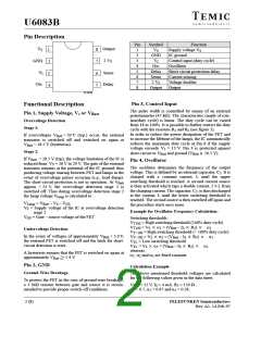
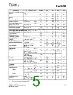
Pin Description
Pin
1
2
3
4
5
6
7
8
Symbol
Function
Supply voltage V
IC ground
Control input (duty cycle)
Oscillator
Short circuit protection delay
Current sensing
Voltage doubler
Output
V
Output
8
7
1
2
3
4
S
V
S
S
GND
2 V
V
I
GND
S
Osc
Delay
Sense
2 V
S
Output
V
Sense
Delay
I
6
5
Osc
95 9944
Pin 3, Control Input
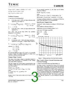
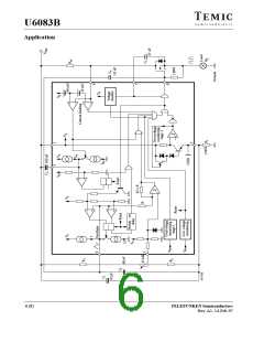
Functional Description
The pulse width is controlled by means of an external
potentiometer (47 k ). The characteristic (angle of rota-
tion/duty cycle) is linear. The duty cycle can be varied
from 18 to 100%. It is possible to further restrict the duty
Pin 1, Supply Voltage, Vs or VBatt
Overvoltage Detection
Stage 1:
cycle with the resistors R and R (see figure 3).
1
2
In order to reduce the power dissipation of the FET and
to increase the lifetime of the lamps, the IC automatically
reduces the maximum duty cycle at Pin 8 if the supply
If overvoltages V
> 20 V (typ.) occur, the external
Batt
transistor is switched off and switched on again at
< 18.5 V (hysteresis).
V
Batt
voltage exceeds V = 13 V. Pin 3 is protected against
2
Stage 2:
short-circuit to V
and ground (V
16.5 V).
Batt
Batt
If V
> 28.5 V (typ), the voltage limitation of the IC is
Batt
Pin 4, Oscillator
reduced from V = 26 V to 20 V. The gate of the external
S
The oscillator determines the frequency of the output
transistor remains at the potential of the IC ground, thus
producing voltage sharing between FET and lamps in the
event of overvoltage pulses occuring (e.g., load dump).
voltage. This is defined by an external capacitor, C . It is
2
charged with a constant current, I, until the upper
switching threshold is reached. A second current source
is then activated which taps a double current, 2 I, from
The short-circuit protection is not in operation. At V
Batt
approx. < 23 V, the overvoltage detection stage 2 is
switched off. Thus during overvoltage detection stage 2
the charging current. The capacitor, C , is thus discharged
2
at the current, I, until the lower switching threshold is
reached. The second source is then switched off again and
the procedure starts once more.
the lamp voltage V
is calculated to :
lamp
V
Lamp
= V – V – V
Batt S GS
V = Supply voltage of the IC at overvoltage detection
S
Example for Oscillator Frequency Calculation:
stage 2
V
GS
= Gate – source voltage of the FET
Switching thresholds
V
V
V
V
V
V
= High switching threshold (100% duty cycle)
T100
= V
= (V
– I
R )
3
T100
S
1
Batt
S
1
Undervoltage Detection
= High switching threshold (< 100% duty cycle)
T<100
T<100
In the event of voltages of approximately V
the external FET is switched off and the latch for short-
circuit detection is reset.
< 5.0 V,
= V
= (V
– I
R )
3
Batt
S
2
Batt
S
2
= Low switching threshold
TL
= V
= (V
– I
R )
3
TL
S
3
Batt
S
3
whereas
and are fixed constant.
A hysteresis ensures that the FET is switched on again at
,
1
2
3
approximately V
5.4 V.
Batt
Pin 2, GND
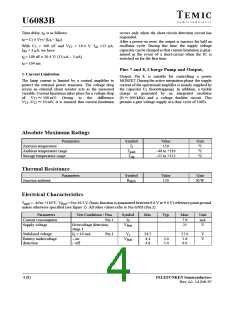
Calculation Example
Ground-Wire Breakage
The above mentioned threshold voltages are calculated
for the following values given in the data sheet.
To protect the FET in the case of ground-wire breakage,
a 1 M resistor between gate and source it is recom-
mended to provide proper switch-off conditions.
V
Batt
= 12 V, I = 4 mA, R = 150
,
S
3
= 0.7, = 0.67 and = 0.28.
1
2
3
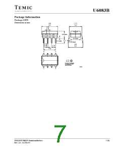
2 (8)
TELEFUNKEN Semiconductors
Rev. A1, 14-Feb-97

 TEMIC [ TEMIC SEMICONDUCTORS ]