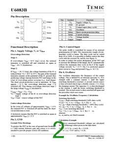
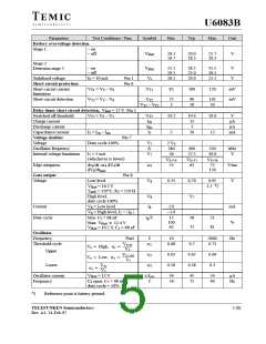
U6083B
V
V
V
= (12 V – 4 mA 150
)
0.7 8 V
Via an external capacitor, C , the slope can be further
reduced as follows:
T100
4
= 11.4 V 0.67 = 7.6 V
T<100
dV /dt = I
/(C + C / )
OSC 4 2 4
8
= 11.4 V 0.28 = 3.2 V
TL
when
I
= 45 A, C = 1.8 nF, C = 68 nF and = 63
OSC
4 2 4
Oscillator Frequency
then dV /dt = 45 A/(1.8 nF + 68 nF/63) = 15.6 V/ms
8
3 cases have to be distinguished
To damp oscillation tendencies, a resistance of 100 in
series with capacitance C is recommended.
1)
f for duty cycle = 100%, no slope reduction with
1
4
capacitor C (see figure 3)
4
Interference Suppression
Iosc
f1
, whereas C2
68 nF
“On board” radio reception according to VDE 0879 part
3/4.81
(
)
2
VT100 VTL
C2
Iosc
45 A
Test conditions refering to figure 2.
f1
...
75 Hz
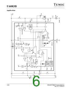
Application circuit according to figure 1 or 3.
Load: nine 4-W lamps in parallel.
Duty cycle = 18%
2)
f for duty cycle < 100%, no slope reduction with
2
capacitor C
4
For a duty cycle of less than 100%, the oscillator
frequency, f, is as follows:
V
Batt
= 12 V
f
= 100 Hz
Osc
Iosc
f2
, whereas C2
Iosc
68 nF
45
2
VT
VTL
C2
100
A
f2
...
69Hz
3)
f with duty cycle < 100% with slope reduction
3
capacitor C (see page 3 “Output Slope Control”)
4
Iosc
f3
(
)
2
VT
VTL
C2 2VBatt C4
100
whereas C2
68 nF
C4
1.8 nF
Iosc
45
A
f3
...
70 Hz
By selecting different values of C and C , it is possible
2
4
to have a range of oscillator frequency, f, from 10 to
2000 Hz as shown in the data sheet.
Output Slope Control
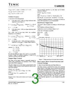
Figure 2. Voltage spectrum of on-board radio reception
The slope of the lamp voltage is internally limited to
reduce radio interference, by limitation of the voltage
gain of the PWM comparator.
Pins 5 and 6, Short-Circuit Protection and
Current Sensing,
Thus the voltage rise on the lamp is proportional to the
oscillator voltage increase at the switchover time accord-
ing to the equation.
1. Short-Circuit Detection and Time Delay, t
d
The lamp current is monitored by means of an external
shunt resistor. If the lamp current exceeds the threshold
dV /dt =
dV /dt =
for the short-circuit detection circuit (V
90 mV), the
duty cycle is switched over to 100% and the capacitor C
8
4
f
4
T2
2
(
–
)
(V
– I
R )
3
4
2
3
Batt
S
5
when
is charged by a current source of I – I . The external
ch dis
f = 75 Hz, V = V
and = 63
FET is switched off after the cut-off threshold (V ) is
TX
T < 100
4
T5
we obtain
reached. Renewed switching on of the FET is possible
only after a power-on reset. The current source, I
dis,
dV8/dt=2 63 75 Hz (0.67–0.28) (12 V–4 mA 15
= 42 V/ms
)
ensures that the capacitor C is not charged by parasitic
currents.
5
TELEFUNKEN Semiconductors
3 (8)
Rev. A1, 14-Feb-97

 TEMIC [ TEMIC SEMICONDUCTORS ]