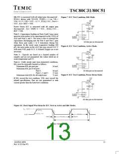
TSC80C31/80C51
* Notice
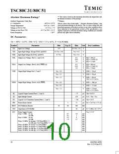
Absolute Maximum Ratings*
Stresses at or above those listed under “ Absolute Maximum Ratings”
may cause permanent damage to the device. This is a stress rating only
and functional operation of the device at these or any other conditions
above those indicated in the operational sections of this specification is
not implied. Exposure to absolute maximum rating conditions may affect
device reliability.
Ambient Temperature Under Bias :
C = Commercial . . . . . . . . . . . . . . . . . . . . . . . . . . . . . . . . 0°C to 70°C
I = Industrial . . . . . . . . . . . . . . . . . . . . . . . . . . . . . . . . . –40°C to 85°C
Storage Temperature . . . . . . . . . . . . . . . . . . . . . . . . –65°C to + 150°C
Voltage on VCC to VSS . . . . . . . . . . . . . . . . . . . . . . . . –0.5 V to + 7 V
Voltage on Any Pin to VSS . . . . . . . . . . . . . . . –0.5 V to VCC + 0.5 V
Power Dissipation . . . . . . . . . . . . . . . . . . . . . . . . . . . . . . . . . . . 1 W**
** This value is based on the maximum allowable die temperature and
the thermal resistance of the package
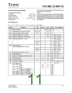
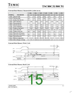
DC Characteristics : Low Power Version
TA = 0°C to 70°C ; Vcc = 2.7 V to 5.5 V ; Vss = 0 V ; F = 0 to 20 MHz
TA = –40°C to 85°C ; Vcc = 2.7 V to 5.5 V ; F = 0 to 20 MHz
Symbol
VIL
Parameter
Min
Typ (3)
Max
Unit
V
Test Conditions
Input Low Voltage
– 0.5
0.2 V – 0.1
CC
VIH
Input High Voltage (Except XTAL and RST)
Input High Voltage to RST for Reset
Input High Voltage to XTAL1
0.2 V + 0.9
V
V
V
+ 0.5
+ 0.5
+ 0.5
V
CC
CC
CC
CC
VIH2
VIH1
VPD
0.7 V
0.7 V
2.0
V
CC
CC
V
Power Down Voltage to Vcc in PD Mode
Output Low Voltage (Ports 1, 2, 3) (4)
5.5
V
VOL
0.45
0.45
V
IOL = 0.8 mA (2)
IOL = 1.6 mA (2)
VOL1 Output Low Voltage Port 0, ALE, PSEN (4)
VOH Output High Voltage (Port 1, 2 and 3)
V
0.9 Vcc
0.9 Vcc
V
V
IOH = – 10 µA
IOH = – 40 µA
VOH1 Output High Voltage (Port 0 in External Bus Mode),
ALE, PSEN
IIL
ILI
Logical 0 Input Current Ports 1, 2, 3
Input Leakage Current
– 50
± 10
– 650
30
µA
µA
µA
µA
Vin = 0.45 V
0.45 < Vin < V
Vin = 2.0 V
CC
ITL
IPD
Logical 1 to 0 Transition Current (Ports 1, 2, 3)
Power Down Current
5
V
= 2.0 V to 5.5 V
CC
(1)
RRST RST Pulldown Resistor
CIO Capacitance of I/O Buffer
50
90
200
10
kΩ
pF
fc = 1 MHz, T = 25_C
A
Icc (mA)
Operating (1)
Idle (1)
2.7 V
3 V
3.3 V
2.7 V
3 V
3.3 V
Frequency/Vcc
Max
0.8
4
Typ
0.37
2.2
4
Max
1
Typ
0.42
2.5
Max
1.1
6
Typ
0.46
2.7
Max
0.4
1.5
2.5
3
Typ
Max
Typ
0.24
1.4
Max
0.6
2
Typ
0.27
1.6
2.6
3
1 MHz
6 MHz
0.22
1.2
1.7
1.9
0.5
1.7
3
5
12 MHz
16 MHz
8
10
12
4.7
12
5.3
2.2
3.5
4.5
10
5
5.8
14
6.6
3.8
2.5
Freq > 12MHz (Vcc = 5.5 V)
Icc op max (mA) = 0.9 × Freq (MHz) + 5
Icc Idle max (mA) = 0.3 × Freq (MHz) + 1.7
12
MATRA MHS
Rev. E (14 Jan.97)

 TEMIC [ TEMIC SEMICONDUCTORS ]