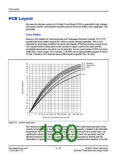
PCB Layout
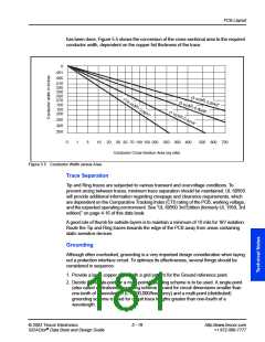
has been done, Figure 5.5 shows the conversion of the cross-sectional area to the required
conductor width, dependent on the copper foil thickness of the trace.
0
.001
.005
.010
.020
.030
.050
.070
.100
.150
.200
.250
.300
.350
0
1
5
10
20 30 50 70 100 150 200 250 300 400
Conductor Cross-Section Area (sq mils)
500 600 700
Figure 5.5 Conductor Width versus Area
Trace Separation
Tip and Ring traces are subjected to various transient and overvoltage conditions. To
prevent arcing between traces, minimum trace separation should be maintained. UL 60950
will provide additional information regarding creepage and clearance requirements, which
are dependent on the Comparative Tracking Index (CTI) rating of the PCB, working voltage,
and the expected operating environment. See "UL 60950 3rd Edition (formerly UL 1950, 3rd
edition)" on page 4-16 of this data book.
A good rule of thumb for outside layers is to maintain a minimum of 18 mils for 1kV isolation.
Route the Tip and Ring traces towards the edge of the PCB away from areas containing
static sensitive devices.
Grounding
Although often overlooked, grounding is a very important design consideration when laying
out a protection interface circuit. To optimize its effectiveness, several things should be
considered in sequence:
1. Provide a large copper plane with a grid pattern for the Ground reference point.
2. Decide if a single-point or a multi-point grounding scheme is to be used. A single-point
(also called centralized) grounding scheme is used for circuit dimensions smaller than
one-tenth of a wavelength (ꢄ = 300,000/frequency) and a multi-point (distributed)
grounding scheme is used for circuit trace lengths greater than one-fourth of a
wavelength.
© 2002 Teccor Electronics
5 - 19
http://www.teccor.com
+1 972-580-7777
®
SIDACtor Data Book and Design Guide

 TECCOR [ TECCOR ELECTRONICS ]