ICM-20690
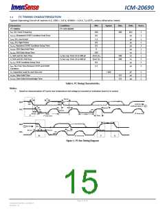
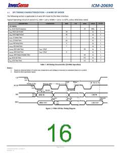
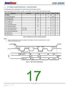
3.5 SPI TIMING CHARACTERIZATION – 4-WIRE SPI MODE
The following section is applicable to 4-wire SPI mode for the Main Interface.
Typical Operating Circuit of section 4.2, VDD = 1.8 V, VDDIO = 1.8 V, TA=25°C, unless otherwise noted.
NOTES
PARAMETERS
CONDITIONS
MIN
TYP
MAX
UNITS
SPI TIMING
fSPC, SCLK Clock Frequency
tLOW, SCLK Low Period
tHIGH, SCLK High Period
tSU.CS, CS Setup Time
10
MHz
ns
ns
ns
ns
ns
ns
ns
ns
ns
ns
ns
1
1
1
1
1
1
1
1
1
1
2
2
56
56
2
tHD.CS, CS Hold Time
63
3
tSU.SDI, SDI Setup Time
tHD.SDI, SDI Hold Time
tVD.SDO, SDO Valid Time
tHD.SDO, SDO Hold Time
tDIS.SDO, SDO Output Disable Time
tFall, SCLK Fall Time
7
Cload = 20 pF
Cload = 20 pF
40
6
20
6.5
6.5
tRise, SCLK Rise Time
Table 7. SPI Timing Characteristics (10-MHz Operation)
Notes:
1. Based on characterization of 5 parts over temperature and voltage as mounted on evaluation board or in sockets
2. Based on other parameter values
CS
70%
30%
tFall
tRise
tHD;CS
tSU;CS
70%
tHIGH
1/fCLK
SCLK
30%
tSU;SDI
tHD;SDI
tLOW
70%
30%
SDI
LSB IN
MSB IN
tDIS;SDO
tVD;SDO
tHD;SDO
70%
30%
SDO
MSB OUT
LSB OUT
Figure 2. 4-Wire SPI Bus Timing Diagram
Page 16 of 76
Document Number: DS-000178
Revision: 1.0

 TDK [ TDK ELECTRONICS ]