HV9910
Application Information
voltage to the LD pin. When soft start is required, a capacitor
can be connected to the LD pin to allow this voltage to ramp
at a desired rate, therefore, assuring that output current of
the LED ramps gradually.
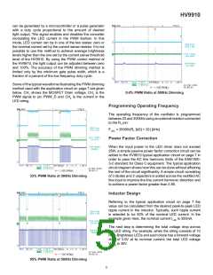
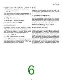
AC/DC Off-Line Applications
The HV9910 is a low-cost off-line buck or boost converter
control IC specifically designed for driving multi-LED stings
or arrays. It can be operated from either universal AC line
or any DC voltage between 8-450V. Optionally, a passive
power factor correction circuit can be used in order to pass
the AC harmonic limits set by EN 61000-3-2 Class C for
lighting equipment having input power less than 25W. The
HV9910 can drive up to hundreds of High-Brightness (HB)
LEDs or multiple strings of HB LEDs. The LED arrays can
be configured as a series or series/parallel connection. The
HV9910 regulates constant current that ensures controlled
brightness and spectrum of the LEDs, and extends their
lifetime. The HV9910 features an enable pin (PWM_D) that
allows PWM control of brightness.
Optionally, a simple passive power factor correction circuit,
consisting of 3 diodes and 2 capacitors, can be added as
shown in the typical application circuit diagram of Figure 1.
Supply Current
A current of 1mA is needed to start the HV9910. As shown
in the block diagram on page 3, this current is internally
generated in the HV9910 without using bulky startup resistors
typically required in the offline applications. Moreover, in
many applications the HV9910 can be continuously powered
using its internal linear regulator that provides a regulated
voltage of 7.5V for all internal circuits.
The HV9910 can also control brightness of LEDs by
programming continuous output current of the LED driver
(so-called linear dimming) when a control voltage is applied
to the LD pin.
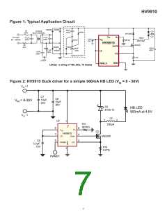
Setting Light Output
When the buck converter topology of Figure 2 is selected,
the peak CS voltage is a good representation of the average
current in the LED. However, there is a certain error
associated with this current sensing method that needs to
be accounted for. This error is introduced by the difference
between the peak and the average current in the inductor.
For example if the peak-to-peak ripple current in the inductor
is 150mA, to get a 500mA LED current, the sense resistor
should be 250mV/(500mA+ 0.5*150mA) = 0.43Ω.
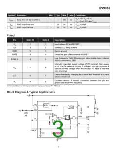
The HV9910 is offered in a standard 8-pin SOIC package. It
is also available in a high voltage rated SO-16 package for
applications that require VIN greater than 250V.
TheHV9910includesaninternalhigh-voltagelinearregulator
that powers all internal circuits and can also serve as a bias
supply for low voltage external circuitry.
LED Driver Operation
Dimming
TheHV9910cancontrolallbasictypesofconverters, isolated
or non-isolated, operating in continuous or discontinuous
conductionmode.Whenthegatesignalenhancestheexternal
power MOSFET, the LED driver stores the input energy in an
inductor or in the primary inductance of a transformer and,
depending on the converter type, may partially deliver the
energy directly to LEDs The energy stored in the magnetic
component is further delivered to the output during the off-
cycle of the power MOSFET producing current through the
string of LEDs (Flyback mode of operation).
Dimming can be accomplished in two ways, separately or
combined, depending on the application. Light output of the
LED can be controlled either by linear change of its current,
or by switching the current on and off while maintaining it
constant. The second dimming method (so-called PWM
dimming) controls the LED brightness by varying the duty
ratio of the output current.
The linear dimming can be implemented by applying a
control voltage from 0 to 250mV to the LD pin. This control
voltage overrides the internally set 250mV threshold level
of the CS pin and programs the output current accordingly.
For example, a potentiometer connected between V and
ground can program the control voltage at the CDSD pin.
Applying a control voltage higher than 250mV will not change
the output current setting. When higher current is desired,
select a smaller sense resistor.
When the voltage at the VDD pin exceeds the UVLO threshold
the gate drive is enabled. The output current is controlled
by means of limiting peak current in the external power
MOSFET. A current sense resistor is connected in series
with the source terminal of the MOSFET. The voltage from
the sense resistor is applied to the CS pin of the HV9910.
When the voltage at CS pin exceeds a peak current sense
voltage threshold, the gate drive signal terminates, and the
power MOSFET turns off. The threshold is internally set
to 250mV, or it can be programmed externally by applying
The PWM dimming scheme can be implemented by applying
an external PWM signal to the PWM_D pin. The PWM signal
4

 SUPERTEX [ Supertex, Inc ]