HV9910
Ordering Information
Package Options
SOIC-16 SOIC-8
HV9910NG-G HV9910LG-G
Device
HV9910
-G indicates package is RoHS compliant (‘Green’)
Absolute Maximum Ratings
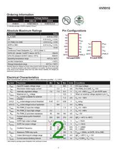
Pin Configurations
Parameter
VIN to GND
CS
Value
NC
VIN
NC
NC
CS
-0.5V to +470V
-0.3V to (VDD + 0.3V)
-0.3V to (VDD - 0.3V)
-0.3V to (VDD + 0.3V)
13.5V
NC
ROSC
LD
LD, PWM_D to GND
GATE to GND
VDDMAX
VIN
CS
ROSC
LD
GND
NC
VDD
NC
Continuous Power Dissipation (TA = +25°C) (Note 1)
16-Pin SO (derate 7.5mW/°C above +25°C)
8-Pin SO (derate 6.3mW/°C above +25°C)
Operating temperature range
GND
GATE
VDD
NC
NC
750mW
630mW
PWM_D
GATE
PWM_D
8-Lead SOIC
16-Lead SOIC
-40°C to +85°C
+125°C
Junction temperature
Storage temperature range
-65°C to +150°C
Absolute Maximum Ratings are those values beyond which damage to the device may
occur. Functional operation under these conditions is not implied. Continuous operation
of the device at the absolute rating level may affect device reliability. All voltages are
referenced to device ground.
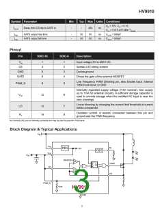
Electrical Characteristics
(Over recommended operating conditions unless otherwise specified - TA = 25°C)
Symbol
VINDC
IINsd
Parameter
Min
8.0
-
Typ
Max
450
1
Units Conditions
Input DC supply voltage range
Shut-down mode supply current
Internally regulated voltage
Maximal pin VDD voltage
V
mA
V
DC input voltage
Pin PWM_D to GND, VIN = 8V
0.5
7.5
-
VDD
7.0
-
8.0
13.5
VIN = 8 – 450V, IDD(ext) = 0, pin GATE open
When an external voltage applied to pin VDD
VDDmax
V
VDD current available for external
IDD(ext)
-
-
1.0
mA
VIN = 8 – 100V
circuitry 1
UVLO
∆UVLO
VEN(lo)
VEN(hi)
REN
VDD undervoltage lockout threshold
VDD undervoltage lockout hysteresis
Pin PWM_D input low voltage
6.45
-
6.7
500
-
6.95
-
V
mV
V
VIN rising
VIN falling
-
1.0
-
VIN = 8 – 450V
VIN = 8 – 450V
VEN = 5V
Pin PWM_D input high voltage
2.4
50
-
V
Pin PWM_D pull-down resistance
100
150
kΩ
Current sense pull-in threshold
voltage
VCS(hi)
225
250
275
mV
@TA = -40°C to +85°C
VGATE(hi)
VGATE(lo)
GATE high output voltage
VDD-0.3
0
-
-
VDD
0.3
V
V
IOUT = 10mA
IOUT = -10mA
GATE low output voltage
20
80
25
100
30
120
kHz
kHz
R = 1.00MΩ
RTT = 226kΩ
fOSC
Oscillator frequency
DMAXhf
VLD
Maximum PWM duty cycle
-
0
-
-
100
250
280
%
mV
ns
FPWMhf = 25kHz, at GATE, CS to GND.
@TA = <85°C, VIN = 12V
Linear dimming pin voltage range
TBLANK
Current sense blanking interval
150
215
VCS = 0.55VLD, VLD = VDD
1 Also limited by package power dissipation limit, whichever is lower.
2

 SUPERTEX [ Supertex, Inc ]