HV9910
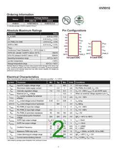
Symbol Parameter
Min
Typ Max Units Conditions
VIN = 12V, VLD = 0.15,
tDELAY
Delay from CS trip to GATE lo
-
-
300
ns
VCS = 0 to 0.22V after TBLANK
tRISE
tFALL
GATE output rise time
GATE output fall time
-
-
30
30
50
50
ns
ns
CGATE = 500pF
CGATE = 500pF
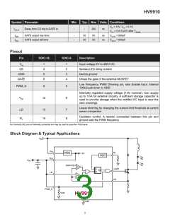
Pinout
Pin
SOIC-16
SOIC-8
Description
VIN
CS
1
4
5
8
1
2
3
4
Input voltage 8V to 450V DC
Senses LED string current
Device ground
GND
GATE
Drives the gate of the external MOSFET
Low Frequency PWM Dimming pin, also Enable input. Internal
100kΩ pull-down to GND
PWM_D
9
5
Internally regulated supply voltage (7.5V nominal). Can supply
up to 1mA for external circuitry. A sufficient storage capacitor is
used to provide storage when the rectified AC input is near the
zero crossings.
VDD
12
6
Linear dimming by changing the current limit threshold at current
sense comparator
LD
RT
13
14
7
8
Oscillator control. A resistor connected between this pin and
ground sets the PWM frequency.
No Connects (NC) are not internally connected and may be used for pass-thru PCB traces.
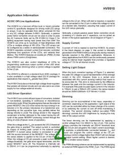
Block Diagram & Typical Applications
V
IN
V
IN
R
T
REG
7.5V
OSC
V
DD
V
DD
250mV
CM
CM
GATE
CS
S
R
Q
LD
PWM_D
100k
HV9910
GND
3

 SUPERTEX [ Supertex, Inc ]