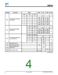
SMS44
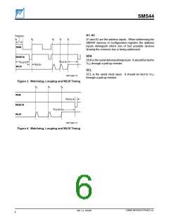
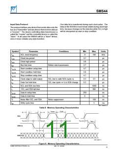
Longdog timer will generally be programmed to be of When the Longdog times out, a reset will be generated.
longer duration than the watchdog and it will generate a When reset returns high (after tPRTO or after a WLDI
resetifittimesout. Bothtimersareclearedbyalowtohigh strobe)bothtimersareresettotimezero. Therefore, ifthe
transition on WLDI and they both start simultaneously.
Longdog tPLDTO is equal to or shorter than the watchdog
tPWDTO, the reset will effectively clear the interrupt before
it can drive the output low.
If the watchdog should timeout the device status will be
recorded in the status register. If the Longdog times out
RESET#willdriveloweitheruntilaWLDIclearisreceived
or until tPRTO (whichever occurs first), at which time it will
return high. Refer to Figures 3 and 4 illustrating the action
of RESET# and IRQ# with respect to the Watchdog and
Longdog timers and the WLDI input.
7
M S B
0
LS B
6
5
4
3
2
1
PU P# S tate
PU P#2
A ddress
S elec t
PU P#3
PU P#1
Loc k A S 0
1
0
1
0
1
0
If WLDI is held low the timers will free-run generating a
series of interrupts and resets. If WLDI is held high the
interrupt (watchdog) output will be disabled and only the
reset (Longdog) output will be active.
Device type address 1010, responds
only to biased A2 & A1 combinations
x
x
0
1
Device type address 1011, responds
only to biased A2 & A1 combinations
0
1
x
x
Configuration read/write enabled
7
M S B
0
LS B
Configuration read/write locked out
6
5
4
3
2
1
2047 Table06 1.0
Table 6.
Conf i gurati on Regi ster 7
SEQ RTO1 RTO0 LD1 LD0 WD2 WD1 WD0
x
x
x
x
x
x
x
x
0
1
x
x
x
x
0
0
1
1
x
x
x
x
x
x
0
1
0
1
x
x
0
0
1
1
x
x
x
x
x
x
0
1
0
1
x
x
x
x
x
x
Longdog Off
1600ms
Register 6 is also used to set the programmable reset
timeout period (tPRTO) and to select the sequence option.
3200ms
6400ms
Bit 1
Bit0
tPDLYX
tPRTO = 25ms
tPRTO = 50ms
tPRTO = 100ms
tPRTO = 200ms
Sequence On
Sequence Off
0
0
1
1
0
1
0
1
0ms (no) Delay
25ms Delay
50ms Delay
100ms Delay
2047 Table07 1.0
Table 7.
PUP Delay s
2047 Table04 1.0
Sequence Delay Programmi ng
Table 4.
Conf i gurati on Regi ster 6
The sequence delays are programmed in register 7. Bit 7
of register 6, must be set to a “0” in order to enable the
sequencing of the PUP# outputs. Sequencing will not
commence until V0 is above its programmed threshold.
7
M S B
0
LS B
6
5
4
3
2
1
SEQ RTO1 RTO0 LD1 LD0 WD2 WD1 W D0
Each PUP# (-3, -2 and -1) is delayed according to the
states of its Bit 1 and Bit 0 as indicated in Table 7.
OFF
0
0
1
1
1
1
0
1
0
0
1
1
0
1
0
1
0
1
400ms
800ms
1600ms
3200ms
6400ms
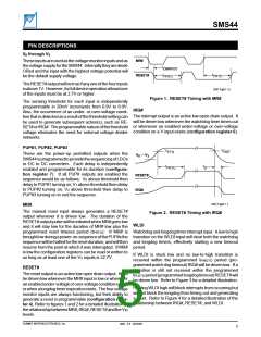
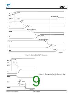
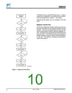
RefertoFigures5and6forthedetailedtimingrelationship
of the programmable power-on sequencing.
2047 Table05 1.0
Table 5.
Conf i gurati on Regi ster 6
SUMMIT MICROELECTRONICS, Inc.
2047 2.3 10/23/00
8

 SUMMIT [ SUMMIT MICROELECTRONICS, INC. ]