SMS44
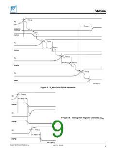
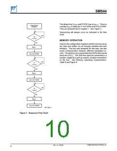
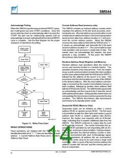
The delay from VPTH0 until PUP#1 low is tPDLY1. There is
a similar tPDLYX delay for V1 to PUP#2 and V2 to PUP#3.
They are programmed in register 7. See Figure 5.
Sequencing
Enabled
Sequencing will always occur as indicated in the flow
chart.
No
V
0
>V
?
PTH
MEMORY OPERATI ON
Yes
Data for the configuration registers and the memory array
are read and written via an industry standard two-wire
interface. The bus was designed for two-way, two-line
serial communication between different integrated cir-
cuits. Thetwolinesareaserialdataline(SDA)andaserial
clock line (SCL). The SDA line must be connected to a
positive supply by a pull-up resistor, located somewhere
on the bus. See Memory Operating Characteristics:
Table 8 and Figure 8.
tPDLY1
Turn On PUP#1
No
V1
>V
?
PTH
Yes
tPDLY2
Turn On PUP#2
No
V2
>V
?
PTH
Yes
tPDLY3
Turn On PUP#3
2047 Fig07 2.1
Fi gure 7.
Sequence Flow Chart
SUMMIT MICROELECTRONICS, Inc.
2047 2.3 10/23/00
10

 SUMMIT [ SUMMIT MICROELECTRONICS, INC. ]