SMS44
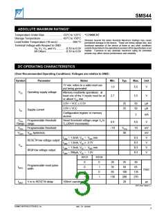
ABSOLUTE MAXI MUM RATI N GS*
Temperature Under Bias ....................... -55°C to 125°C *COMMENT
Storage Temperature ............................ -65°C to 150°C
Lead Solder Temperature (10 secs) ................... 300 °C
Terminal Voltage with Respect to GND:
Stresses beyond the listed Absolute Maximum Ratings may cause
permanent damage to the device. These are stress ratings only, and
functional operation of the device at these or any other conditions
outside those listed in the operational sections of this specification is not
implied. Exposure to any absolute maximum rating for extended
periods may affect device performance and reliability.
V , V , V , and V ........... -0.3V to 6.0V
0
1
2
3
All Others ........................ -0.3V to 6.0V
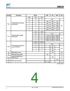
DC OPERATI NG CHARACTERI STI CS
(Over Recommended Operati ng Condi ti ons; Voltages are relati ve to GN)D
Sym bol
Param eter
Notes
Min.
Typ.
Max.
U nti
1V min. refers to a valid reset out-
put being generated
1.0
5.5
V
VCC
Operating supply voltage
Memory read/write operations: at
least one of the V inputs must be at
or above VCC min.
2.7
5.5
V
3.6V < VCC ≤ 5.5V
3.6V ≥ VCC
25
25
50
50
µA
µA
ICC
Supply current
Configuration register or memory
access
2
mA
V
VPTH
Programmable threshold
Reset threshold voltage range V0 to
V3 (20mV increments)
0.9
6.0
10
Range range
VPTH
Programmable threshold
–10
VPTH
50
mV
mV
V
VHYST VRST hysteresis
ISINK = 1.2mA, VCC = VRST min.
0.3
0.3
0.3
0.3
RESET# low voltage output
ISINK = 1.2mA, VCC ≥ 2.7V
ISINK = 1.2mA, VCC = VRST min.
ISINK = 200µA, VCC = 1.2V
V
VOL
V
IRQ# low voltage output
V
RTO1
RTO0
0
0
1
1
0
1
0
1
20
35
25
50
30
65
Programmable reset pulse
width
tPRTO
msec
µs
65
100
200
20
135
270
130
tDRST
V in to RESET# delay
100mV overdrive
2047 Elect TableA 2.1
SUMMIT MICROELECTRONICS, Inc.
2047 2.3 10/23/00
3

 SUMMIT [ SUMMIT MICROELECTRONICS, INC. ]