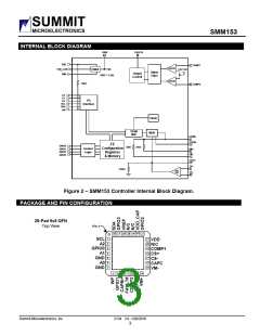
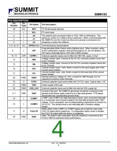
SMM153
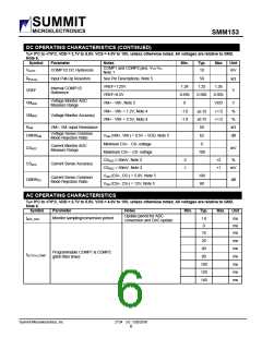
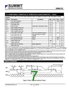
I2C 2-WIRE SERIAL INTERFACE AC OPERATING CHARACTERISTICS – 100kHz
TA= 0°C to +70°C, VDD = 2.7V to 5.5V unless otherwise noted. All voltages are relative to GND. See Figure 3 Timing
Diagram.
Symbol Description
Conditions
Min Typ
Max Units
fSCL
SCL Clock Frequency
0
100
KHz
tLOW
Clock Low Period
4.7
4.0
4.7
4.7
4.0
4.7
0.2
μs
μs
μs
μs
μs
μs
μs
tHIGH
tBUF
Clock High Period
Bus Free Time
Before New Transmission, Note 5
tSU:STA
tHD:STA
tSU:STO
tAA
Start Condition Setup Time
Start Condition Hold Time
Stop Condition Setup Time
Clock Edge to Data Valid
SCL low to valid SDA (cycle n)
3.5
SCL low (cycle n+1) to SDA
change
tDH
Data Output Hold Time
0.2
μs
tR
SCL and SDA Rise Time
SCL and SDA Fall Time
Data In Setup Time
Note 5
Note 5
1000
300
ns
ns
ns
ns
ns
ms
tF
tSU:DAT
tHD:DAT
TI
250
0
Data In Hold Time
Noise Filter SCL and SDA
Write Cycle Time
Noise suppression
100
tWR
5
Note 1: VHYST is measured with a 1.25V external voltage and is determined by subtracting Threshold Low from Threshold High, VTH-VTL while monitoring
the FAULT# pin state. Actual DC Hysteresis is derived from the equation: (VIN(COMP1/2)/VREF)(VHYST). For example, if VIN(COMP1/2)/=2.5V and VREF=1.25V then
Actual DC Hysteresis= (2.5V/1.25V)(0.003V)=6mV.
Note 2: Current sense accuracy depends on the current sense resistor tolerance. Kelvin sensing of the voltage drop across this resistor must be used to
guarantee accuracy. Accuracy at the low range of the current monitor ADC will be adversely impacted by offset errors.
Note 3: It is recommended that ADC reads occur with a frequency of not more than 250Hz.
Note 4: Voltage accuracy is only guaranteed for factory-programmed settings. Changing voltage from the value reflected in the customer specific CSIR
code may result in inaccuracies exceeding those specified above.
Note 5: Not 100% Production tested. Guaranteed by Design and/or characterization.
Note 6: All electrical parameters are guaranteed to function over the stated VDD, VCS and temperature range. Electrical parameters not specified as
"guaranteed by design" are tested with a VDD voltage required of the specific application. For example, if the device is to be operated at 3.3V and VCS
supply of 12V, it is tested with a VDD supply of 3.3V, +-10% and a VCS supply of 12V, +-10%.
TIMING DIAGRAMS
tWR (For Write Operation Only)
tHIGH
tLOW
tR
tF
SCL
tBUF
tHD:DAT
tSU:DAT
tSU:STA
tSU:STO
tHD:STA
SDA (IN)
tAA
tDH
SDA (OUT)
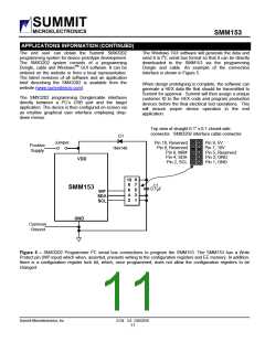
Figure 3. Basic I2C Serial Interface Timing
Summit Microelectronics, Inc
2134 3.0 1/20/2010
7

 SUMMIT [ SUMMIT MICROELECTRONICS, INC. ]