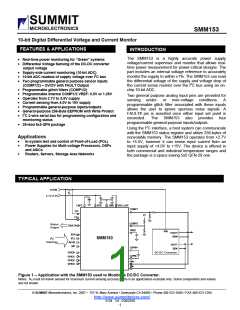
SMM153
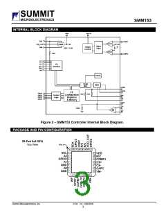
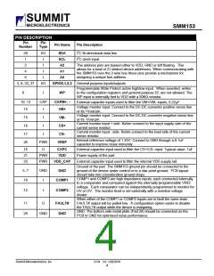
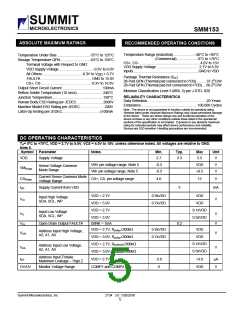
PIN DESCRIPTION
Pin
Number
Pin
Type
Pin Name
Pin Description
28
I/O
SDA
SCL
A2
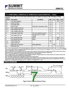
I2C Bi-directional data line
I2C clock input.
1
I
The address pins are biased either to VDD, GND or left floating. This
allows for a total of 21 distinct device addresses. When communicating with
the SMM153 over the 2-wire bus these pins provide a mechanism for
assigning a unique bus address.
2
I
I
4
A1
6
I
A0
3, 9, 22, 27
I/O
GPIO0,1,2,3 General purpose inputs/outputs.
Programmable Write Protect active high/low input. When asserted, writes
to the configuration registers and general purpose EE are not allowed. The
8
I
WP
WP input is internally tied to VDD with a 50KΩ resistor.
10, 13
14
CAP
I
CAPM+, -
VM+
External capacitor inputs used to filter the VM+/VM- inputs, 0.22μF.
Voltage monitor input. Connect to the DC-DC converter positive sense line
or its +Vout pin.
Voltage monitor input. Connect to the DC-DC converter negative sense line
or its -Vout pin.
Current monitor input + side. Kelvin connect to the input supply side of the
current sense resistor.
Current monitor input - side. Kelvin connect to the load side of the current
sense resistor.
Internal reference voltage of 1.25V. Connect to GND through a 0.1uF
capacitor to improve noise immunity.
15
18
17
26
I
VM-
CS+
CS-
I
I
PWR
VREF
16
21
23
O
CAPC
VDD
External capacitor input used to filter the CS+/CS- input. Typical value: 1uF.
Power supply of the part.
PWR
PWR
VDD_CAP
External capacitor input used to filter the internal VDD supply rail.
Ground of the part. The SMM153 ground pin should be connected to the
ground of the device under control or to a star point ground. PCB layout
should take into consideration ground drops.
COMP1 and COMP2 are high impedance inputs, each connected internally
to a comparator and compared against the internally programmable VREF
voltage. Each comparator can be independently programmed to monitor for
UV or OV. The monitor level is set externally with a resistive voltage
divider.
5, 7
19
GND
I
GND
COMP1
12
I
COMP2
When either of the COMP1 or COMP2 inputs are in fault the open-drain
FAULT# output will be pulled low. A configuration option exists to disable
the FAULT# output while the device is margining.
GND. The bottom side metal plate (Pad 29) should be connected on the
PCB to GND for optimized noise performance.
11
29
O
FAULT#
GND
GND
Summit Microelectronics, Inc
2134 3.0 1/20/2010
4

 SUMMIT [ SUMMIT MICROELECTRONICS, INC. ]