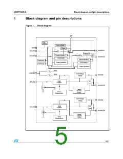
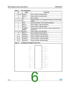
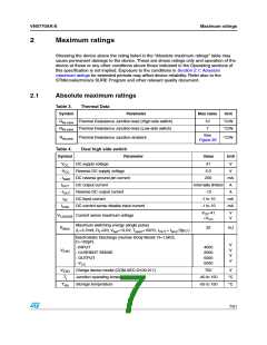
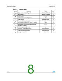
VN5770AK-E
Electrical characteristics
3
Electrical characteristics
3.1
Electrical characteristics for dual high side switch
Note:
Values specified in this section are for 8V < V < 36V; -40°C < T < 150°C, unless
CC
j
otherwise specified (for each channel)
Table 6.
Symbol
Power section
Parameter
Test Conditions
Min. Typ.
Max. Unit
Operating supply
voltage
VCC
VUSD
4.5
13
3.5
0.5
36
V
V
V
Undervoltage
shutdown
4.5
Undervoltage shut-
down hysteresis
VUSDhyst
IOUT=3A; Tj=25°C
Onstate resistance IOUT=3A; Tj=150°C
IOUT=3A; VCC=5V; Tj=25°C
IS=20 mA
160
320
210
mΩ
mΩ
mΩ
RON
Vclamp Clamp Voltage
41
46
52
V
Off State; VCC=13V; Tj=25°C;
VIN=VOUT=VSENSE=0V
IS
Supply current
2(1)
3
5(1)
6
µA
mA
On State; VCC=13V; VIN=5V; IOUT=0A
VIN=VOUT=0V; VCC=13V; Tj=25°C
VIN=VOUT=0V; VCC=13V; Tj=125°C
0
0
3
5
Off state output
current(2)
IL(off)
µA
Output - VCC diode
voltage(2)
VF
-IOUT=3A; Tj=150°C
0.7
V
1. PowerMOS leakage included
2. For each channel
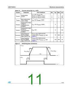
Table 7.
Symbol
td(on)
td(off)
Switching (V =13V)
CC
Parameter
Test Conditions
Min.
Typ.
Max.
Unit
Turn-on delay time RL=4.3Ω (see Figure 3.)
Turn-off delay time RL=4.3Ω (see Figure 3.)
15
10
µs
µs
Turn-on voltage
RL=4.3Ω
See
Figure 15
(dVOUT/dt)on
(dVOUT/dt)off
WON
V/µs
V/µs
mJ
slope
Turn-off voltage
RL=4.3Ω
SeeFigure
slope
17.
Switching energy
RL=4.3Ω (see Figure 3.)
losses during twon
0.16
0.08
Switching energy
WOFF
RL=4.3Ω (see Figure 3.)
losses during twoff
mJ
9/31

 STMICROELECTRONICS [ ST ]