VN5770AK-E
Maximum ratings
2
Maximum ratings
Stressing the device above the rating listed in the “Absolute maximum ratings” table may
cause permanent damage to the device. These are stress ratings only and operation of the
device at these or any other conditions above those indicated in the Operating sections of
this specification is not implied. Exposure to the conditions in Section 2.1: Absolute
maximum ratings for extended periods may affect device reliability. Refer also to the
STMicroelectronics SURE Program and other relevant quality document.
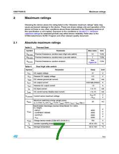
2.1
Absolute maximum ratings
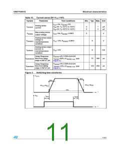
Table 3.
Symbol
Thermal Data
Parameter
Max value
Unit
Rthj-case Thermal Resistance Junction-lead (High-side switch)
Rthj-case Thermal Resistance Junction-lead (Low-side switch)
10
7
°C/W
°C/W
See
Figure 38
Rthj-amb Thermal Resistance Junction-ambient.
°C/W
Table 4.
Symbol
Dual high side switch
Parameter
Value
Unit
VCC
DC supply voltage
41
0.3
V
V
-VCC
Reverse DC supply voltage
- IGND DC reverse ground pin current
IOUT DC output current
- IOUT Reverse DC output current
200
mA
A
Internally limited
-12
A
IIN
DC input current
-1 to 10
-1 to 10
mA
mA
ICSD
DC current sense disable input current
VCC-41
+VCC
V
V
VCSENSE Current sense maximum voltage
Maximum switching energy (single pulse)
EMAX
32
mJ
(L=3.7mH; RL=0Ω; Vbat=13.5V; Tjstart=150ºC; IOUT = IlimL(Typ.) )
Electrostatic Discharge (Human Body Model: R=1.5KΩ;
C=100pF)
V
V
V
V
- INPUT
4000
2000
5000
5000
VESD
- CURRENT SENSE
- OUTPUT
- VCC
VESD
Tj
Charge device model (CDM-AEC-Q100-011)
Junction operating temperature
Storage temperature
750
V
-40 to 150
-55 to 150
°C
°C
Tstg
7/31

 STMICROELECTRONICS [ ST ]